
Index 316
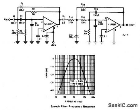
SPEECH_FILTER(300_Hz3_kHz_BANDPASS)
Published:2009/6/30 2:02:00 Author:May
View full Circuit Diagram | Comments | Reading(1129)
Wien_bridge_oscillator_with_common_mode_suppression
Published:2009/7/24 20:36:00 Author:Jessie
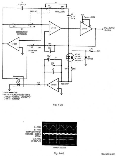
Figure 4-39 shows another version of the Fig. 4-34 circuit, but with automatic trim and common-mode suppression (similar to that of Fig. 4-28). The circuit output (trace A, Fig. 4-40) contains less than 0.0003% (3 ppm) distortion (trace B), with no visible correlation to gain-loop ripple residue (trace C). This level of distortion is below the uncertainty floor of most distortion analyzers. LINEAR TECHNOLOGY, APPLICATION NOTE 43, P. 32, 33. (View)
View full Circuit Diagram | Comments | Reading(644)
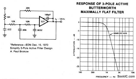
POLE_ACTIVE_LOW_PASS_FILTER(B_UTTERWORTH_MAXIMALLY_FLAT_RESPONSE)
Published:2009/6/30 2:00:00 Author:May
View full Circuit Diagram | Comments | Reading(757)
Wien_bridge_oscillator_with_automatic_trim
Published:2009/7/24 20:35:00 Author:Jessie
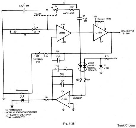
Figure 4-38 shows another version of the Fig. 4-34 circuit, but with automatic trim for distortion. Q1 is replaced with an optically driven CdS photocell, and the LT1055 is replaced with a ground-sensing op amp operating in the single-supply mode. Distortion improves slightly to 0.0015%. LINEAR TECHNQLOGY, APPLICATION NOTE 43, P. 33. (View)
View full Circuit Diagram | Comments | Reading(751)
Wien_bridge_oscillator_with_improved_stabilization
Published:2009/7/24 20:33:00 Author:Jessie
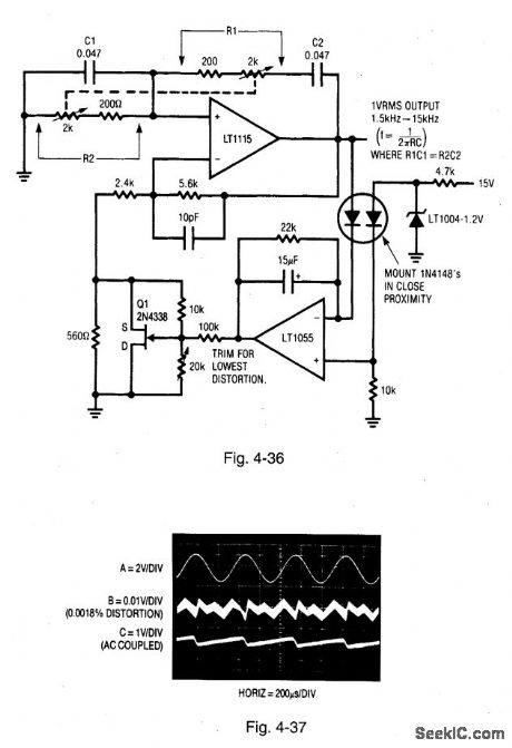
Figure 4-36 shows an improved version of the Fig. 4-34 circuit. Figure 4-37 shows waveforms for the Fig. 4-36 circuit. The 20-kΩ trimmer in the Q1 circuit makes it possible to get 0.0018% distortion (trace B, Fig. 4-37). LINEAR TECHNOLOGY, APPLICATION NOTE 43, P. 31. (View)
View full Circuit Diagram | Comments | Reading(634)
Wien_bridge_sine_wave_oscillator_with_electronic_amplitude_stabilization
Published:2009/7/24 20:31:00 Author:Jessie
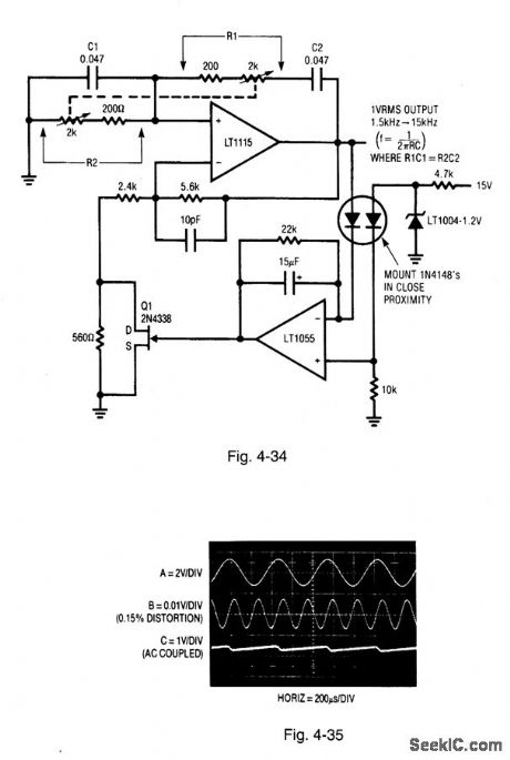
Figure 4-34 shows a sine-wave oscillator that uses electronic stabilization in place of the lamp. Figure 4-35 shows the waveforms. Trace A shows the output. Trace B shows distortion, and trace C shows the rectifier peaking residue at the Q1 gate. LINEAR TECHNOLOGY, APPLICATION NOTE 43, P. 30, 31. (View)
View full Circuit Diagram | Comments | Reading(669)
8_BIT_DIGlTAL_OUTPUT
Published:2009/6/30 1:54:00 Author:May
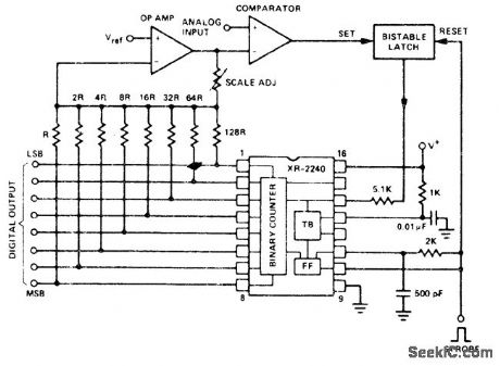
Digital output is obtained in parallel format from binary-counter output of Exar XR-2240 programmable timer/counter. Recycle time is about 6 ms. Supply voltage can be 4-15 V.— Timer Data Book, Exar Integrated Systems, Sunnyvale, CA, 1978, p 11-18. (View)
View full Circuit Diagram | Comments | Reading(1485)
HI_FI_EXPANDER
Published:2009/6/30 1:54:00 Author:May
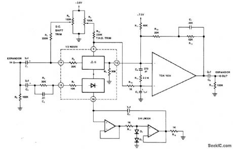
Used in playback of material that has been recorded with overload-prevent ing compressor. Extemal opamp is used for high slew rate. Adjust distortion trimpot Rg for minimum total harmonic distortion-when using input of 0 dBm at 10 kHz. Adjust DC shift pot Re after this, for minimum envelope bounce with tone-burst input,-″Signetics Analog Data Manual,″ Signetics, Sunnyvale,CA,1977,p 804-805. (View)
View full Circuit Diagram | Comments | Reading(960)
Multi_range_Wien_bridge_sine_wave_oscillator
Published:2009/7/24 20:29:00 Author:Jessie
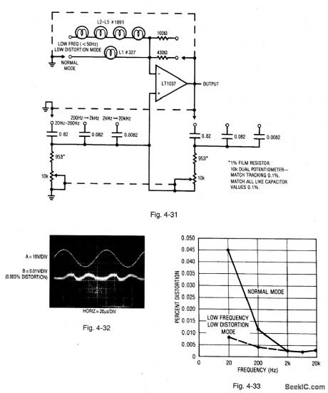
Figure 4-31 shows a Wien-bridge sine-wave oscillator with a frequency range from 20 Hz to 20 kHz, in three decade ranges, with 0.25-dB amplitude flatness. Trace A of Fig. 4-32 shows circuit output at 10 kHz. Trace B shows distortion (below 0.003%). Figure 4-33 plots distortion versus frequency. LINEAR TECHNOLOGY, APPLICATION NOTE 43, P. 29, 30. (View)
View full Circuit Diagram | Comments | Reading(752)
Basic_Wien_bridge_sine_wave_oscillator
Published:2009/7/24 20:27:00 Author:Jessie
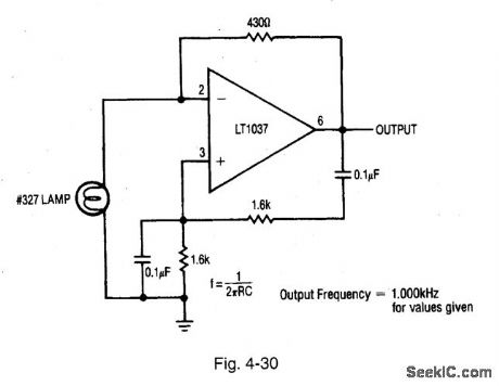
Figure 4-30 shows a Wien-bridge sine-wave oscillator with a lamp in one leg of the bridge(similar to that of Figs,4-26 and 4-28).LINEAR TECHNOLOGY,APPLICATION NOTE 43,P. 29. (View)
View full Circuit Diagram | Comments | Reading(772)
8_BIT_TRACKING
Published:2009/6/30 1:52:00 Author:May
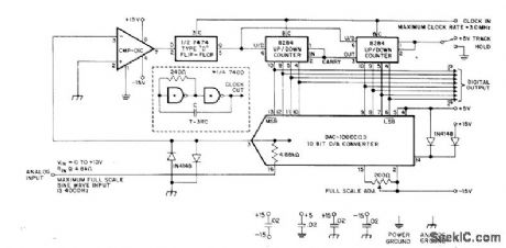
Uses Precision MonolithIcs DAC-100 CCQ3 D/A converter and CMP-01CJ fast precision comparator to make digital data contiguously available at output while tracking analog input. Diode clamps hold DAC output near zero despite input and turn-on transients.Unused least significant digital inputs of 10-bit DAC are turned off by connecting to +5 V as shown. Simple clock circuit shown in dashed box is stable over wide range of temperatures and supply voltages. D/A ionverter is used in feedback configuration to obtain A/D opera-tion.— A Low Cost, High-Performance Tracking A/D Converter, Precision Monolithics, Santa Clara, CA, 1977, AN-6.P 2. (View)
View full Circuit Diagram | Comments | Reading(839)
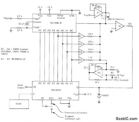
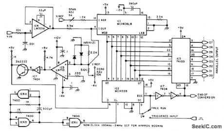
CMOS_COMPATIBLE_SUCCESSIVE_APPROXI_MATION
Published:2009/6/30 1:51:00 Author:May

Converts analog inputto 8-bit digital output by using MC14559 CMOS successive-approximation registerwith Precision Monolithics DAC-100 D/A converter and CMP-01 comparator. Conversion sequence is initiated by applying positive pulse, with width greaterthan one clock cycle, to START CONVERSION input. Analog input is then compared successively to 1/2 scale, 1/4 scale, and remaining binarily decreasing bit weights until it has been resolved within 1/2 LSB. END OF CONVERSION then changes to logic 1 and parallel answer is present in negative-true binary-coded format at register outputs.—D. Soderquist, Interfacing Precision Monolithics Digital-to-Analog Converters with CMOS Logic, Precision Monolithics, Santa Clara, CA, 1975, AN-14, p 4. (View)
View full Circuit Diagram | Comments | Reading(1116)
8_BIT_SUCCESSIVE_APPROXIMATION
Published:2009/6/30 1:48:00 Author:May

Requires only four ICs. For each cycle, most significant bit is enabled first, with comparator giving output signifying that input signal is greater or less in amplitude than output of Motorola MC1408. If output is greater, bit is reset or turned off. Process is repeated for next most significant bit until all bits have been tried, completing conversion cyde. Conversion time is 18 μs, total propagation delay is about 1.5 μs, and ovorall operational figure is about 2 μS per bit for 8-bit system.—T.Henry, Successive Approximation A/D Coversion, Motorola、Phoenix、AZ,1974、AN-716、p 4. (View)
View full Circuit Diagram | Comments | Reading(725)
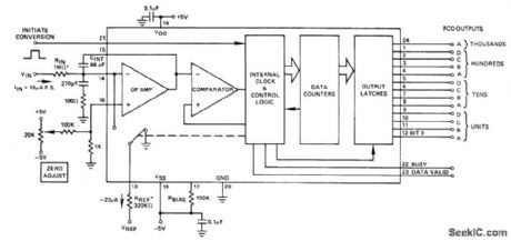
2_DIGIT_BCD
Published:2009/6/30 1:48:00 Author:May
Uses Motorola MC14549 successive-approximation register and MC1408L-8 D/A converter to give full-scale value of 0.99 V in 10-mV increments. Input is buffered by opamp A1 connected as voltage follower, with pot P1 set to give output current proportional to un-known input voltage. This current is compared to that required by total BCD A/D converter. Pins 1-4 and 12-15 of MC14549 provide required 2-digit parallel BCD output. Clock frequency can be 100 kHz.-D. Aldridge, Successive Approximation BCD AiD Converter, Motorola, Phoenix, AZ, 1975, EB-51. (View)
View full Circuit Diagram | Comments | Reading(1589)
BCD_OUTPUT
Published:2009/6/30 1:45:00 Author:May
Latched nonmultiplexed paral lel BCD outputs from Teledyne 8750 3 1/2-digit CMOS analog-to-dighal converter are suitable for liquid crystal and gas-discharge displays. 2-mA drain on 15 V supply permits battery operation. Features include high linearity, noise immunity, and 3 1/2-digit resolution within 0.025% error. Circuit is based on switching number of cument pulses needed to bring analog current to zero at input of opamp, then detarmining digital equivalent by counting these pulses. Values shown are for full-scale voltage input of 10 V and voltage reference of -6.4 V.—CMOS A-D Converter Provides BCD Output, Computer Design, Nov. 1977, p 156 and 158. (View)
View full Circuit Diagram | Comments | Reading(678)
VOICE_DIGITIZER
Published:2009/6/30 1:44:00 Author:May
Uses 8-bit ADC capable of sampling AF input signal 100,000 times per second when using 900-kHz clock. 100-kHz clock gives 9000 samples per second, about minimum for human voice. Digital output is stored in computer memory for later conversion back to analog form for such applications as synthesis of speech from phonemes and providing voice answers to queries. Requires about 10,000 bytes in memory for 1 s of voice data. Pin 7 of IC4 is +12 V, and pin 4 is -6 V. For IC6 and IC7, pin 14 is +5 V and pin 7 is ground. 8080 assembler programs are given for input and output of memory.—S. Ciarcia, Talk to Me! Add a Voice to Your Computerfor $35, BYTE, June 1978, p 142-151. (View)
View full Circuit Diagram | Comments | Reading(1748)
EXTERNAL_TRlGGER
Published:2009/6/30 1:41:00 Author:May
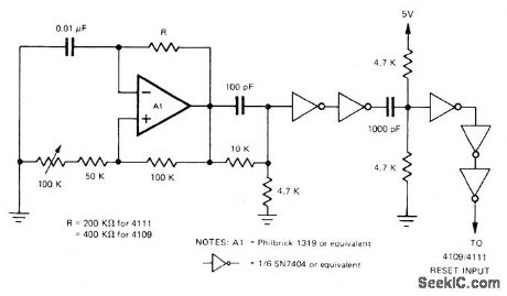
Generates pulse with 100-ns minimum width in range of 125-250 Hz for application to reset input of Teledyne Philbrick A/D converter in applications requiring un attended operation with continuous conversion. Adjust 100K pot to give 125 Hz for 4109 or 250 Hz for 4111. Successive stages of SN7404 inverter provide required sharpening of pulse.A1 is positive-starting MVBR.—R. W. Jacobs, Repetitive Mode Operation for Models 4109/4111 Integrating A/D Converters, Teledyne Philbrick, Dedham, MA, 1977, AN-28. (View)
View full Circuit Diagram | Comments | Reading(875)
SPEECH_FILTER
Published:2009/6/30 1:40:00 Author:May
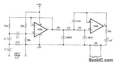
Pair of Bessel-type high-pass filters removes undesired components created by peak clipping during audio signal processing, Developed for use with automatic level control applications of NE571 analog compandor.-W.G. Jung, Gain Control IC for Audio Signal Pro-cessing, Ham Radio, July 1977, p 47-53. (View)
View full Circuit Diagram | Comments | Reading(2300)
BINARY_OUTPUT
Published:2009/6/30 1:38:00 Author:May
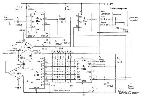
Converts analog signal in range of 0-10 V to 8-bit binary word having all 0s for 0V and all 1s for full-scale input of +9.960V output is 15-V CMOS-compatible but can be adapted for TTL compatibility,Maximum conversion time is about 26 ms. A2 and A3 form negative-going staircase generatof for which startconversion signal is formed by one section of 556. Opamp A4 compares negative output of 7530 with input voltage Vin. When 7530 output voltage equals input voltage, comparator output goes positive and resets control flip-flop to complete gonversion.—W. G. Jung, IC Timer Cookbook, Howard W. Sams, Indianapolis, IN,1977, p 226-228. (View)
View full Circuit Diagram | Comments | Reading(749)
SYMMETRICAL_ACTIVE_CROSSOVER
Published:2009/6/30 1:38:00 Author:May
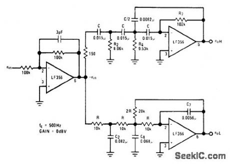
Provides -18dB per octave rolloff (third order) and maximally fiat (Butterworth) characteristics for crossover frequency of 500 Hz. Uses National LF356 opamps in highpass and low-pass filters and same opamp as buffer having low driving impedance required by active filters. Power supplies are ±15V. Design equations are given.- Audio Handbook, National Semiconductor, Santa Clara, CA, 1977, p 5-1-5-7. (View)
View full Circuit Diagram | Comments | Reading(1756)
| Pages:316/471 At 20301302303304305306307308309310311312313314315316317318319320Under 20 |
Circuit Categories
power supply circuit
Amplifier Circuit
Basic Circuit
LED and Light Circuit
Sensor Circuit
Signal Processing
Electrical Equipment Circuit
Control Circuit
Remote Control Circuit
A/D-D/A Converter Circuit
Audio Circuit
Measuring and Test Circuit
Communication Circuit
Computer-Related Circuit
555 Circuit
Automotive Circuit
Repairing Circuit