
Index 311
LOW_DRIFT_SAMPLE_AND_HOLD
Published:2009/6/30 3:22:00 Author:May
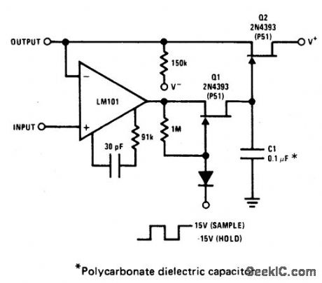
TheJFETs, Q1 and Q2, provide complete buffering to C1, the sample and hold capacitor.During sample, Q1 is turned on and provides a path, rds(on), for charging C1. During hold, Q1 is turned off, thus leaving Q1 ID(off) (<100 pA) and Q2 IGSS (< 100 pA) as the only discharge paths. Q2 serves a buffering function so feedback to the LM101 and output current are supplied from its source. (View)
View full Circuit Diagram | Comments | Reading(2440)
ULTRASONIC_PEST_REPELLER
Published:2009/6/30 3:22:00 Author:May
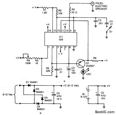
The device emits ultrasonic sound waves that sweep between 65,000 and 25,000 hertz. Designed around a 556 dual timer, one half operated as an astable nultivibrator with an adjustable frequency of 1 to 3 Hz. The second half is also operated as an astable multivibrator but with a fixed free running frequency around 45,000 Hz. The 25-65 kHz sweep is ac-complished by coupling the voltage across C2 (the timing capacitor for the first half of the 556) via Q1 to the control voltage terminal (pin 11) of the second half of the 556. The device that radiates the ultrasonic sound is a piezo tweeter. (View)
View full Circuit Diagram | Comments | Reading(6632)
25_W_logic_indicator_lamp_driver
Published:2009/7/24 11:44:00 Author:Jessie
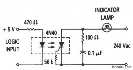
This circuit makes it possible to directly couple (without buffers) TTL and DTL inputs with either indicator or alarm devices. The optoelectronic coupling prevents both logic glitches and the introduction of noise. Motorola Thyristor Device Data, 1989, p. 6-20. (View)
View full Circuit Diagram | Comments | Reading(683)
BELL_SYSTEM_
Published:2009/6/30 3:22:00 Author:May
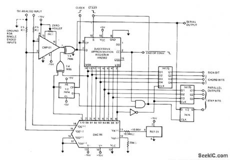
μ-255 COMPANDING LAW—Precision MonolithiCS DAa-86 is used in circuitthat provides 15-segment linear approximation by using 3 bits to select one of eight binarily related chords, then using 4 bits to select one of sixteen Iinearly related steps within each chord.Sign bit determines signal polarity, and encode/decode select bit determines operation, Circuit shown is for palallel data applications Forserialdata,omit inverter, two 74175 chips,and half of 7474 Power supplies should be well by-passed,— COMDAC Companding D/A Converter, Precision Monolithics, Santa Clara, GA, 1977, DAC-86,p 6. (View)
View full Circuit Diagram | Comments | Reading(780)
TTL_compatible_solid_state_relay
Published:2009/7/24 11:43:00 Author:Jessie
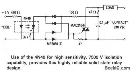
This circuit is compatible with 74, 74S, and 74H series TTL-logic inputs, and can handle 240 Vac loads up to 10 A. Motorola Thyristor Device Data, 1989, p. 6-20. (View)
View full Circuit Diagram | Comments | Reading(1073)
M68000_microcomputer_interface
Published:2009/7/24 11:41:00 Author:Jessie
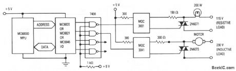
This circuit shows interface between an M68000 and resistive or inductive loads, using MOC3031 and MOC3041 optoisolators. The zero-crossing feature of these optoisolators extends life of incandescent lamps, reduces triac surge-current strains, and reduces EMI, as described for the circuit of Fig. 6-39 (but without the need for a timing circuit at the 7400 gate inputs). Motorola Thyristor Device Data, 1991, p. 1-6-16. (View)
View full Circuit Diagram | Comments | Reading(1949)
M6800_microcomputer_interface
Published:2009/7/24 11:37:00 Author:Jessie
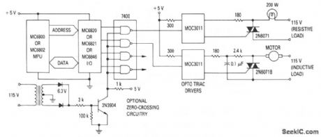
This circuit shows interface between an M6800 or M6802 and resistive or inductive loads. If the second input of the gates is tied to the optional timing circuit shown, the triacs will fire only at the zero crossing of the ac line voltage. This extends life of incandescent lamps, reduces surge-current strains on the triac, and reduces EMI generated by load switching-all without special software or programming within the processor. Motorola Thyristor Device Data, 1991, p. 1-6-14. (View)
View full Circuit Diagram | Comments | Reading(422)
MOS_to_ac_load_interface
Published:2009/7/24 11:33:00 Author:Jessie
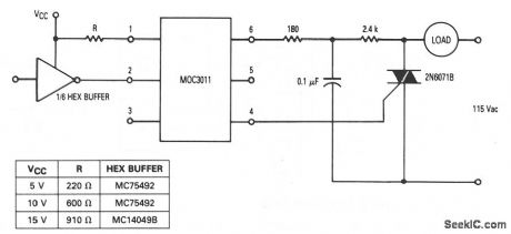
This circuit shows interface between MOS logic and an ac load, using an MOC3011 optoisolator with triac-driver output (chapter 9). The value of R depends on the type of MOS buffer used. Motorola Thyristor Device Data, 1991, p. 1-3-16. (View)
View full Circuit Diagram | Comments | Reading(1789)
Logic_to_inductive_load_interface
Published:2009/7/24 11:31:00 Author:Jessie
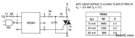
This circuit shows interface between conventional 7400 TTL logic and a triac, using an MOC3011 optoisolator with triac-driver output (chapter 9). The values of C and R2 depend on the triac current. Maxim, 1992, Appications and Product Highlights, p. 1-3-15. (View)
View full Circuit Diagram | Comments | Reading(768)
Fully_isolated_data_MUX
Published:2009/7/24 11:30:00 Author:Jessie
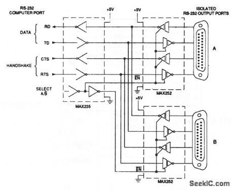
This fully-isolated RS-232 MUX allows a single RS-232 computer port, powered from 5 V, to drive one of two separate remotely located peripherals (typically a data-acquisition satellite and a remote printer). Isolation is useful here because both devices are likely to have ground potentials different from that of the computer. Also, the connection isolates the peripherals from each other as well as the computer. The MAX235 takes RS-232 data and handshake lines and a Select A/B output from the computer and converts them to logic levels. These levels are passed along to both MAX252 isolated transceivers. The RTS line controls which port is selected. Maxim, 1992,Appications and Product Highlights, p. 2-8. (View)
View full Circuit Diagram | Comments | Reading(1558)
Two_RS_232_serial_ports_with_one_chip
Published:2009/7/24 11:27:00 Author:Jessie
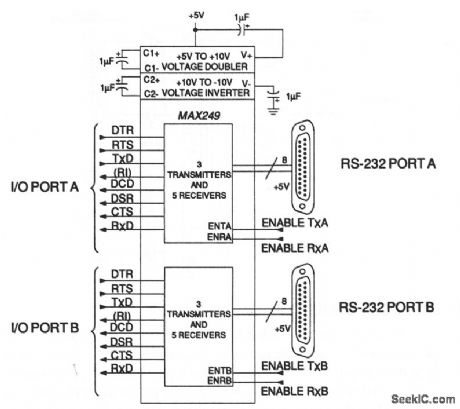
In this circuit, a MAX249 includes a full complement of drivers and receivers for two complete DTE (Data Terminal Equipment) serial ports. The circuit also saves power with separate shutdown inputs for the inputs and outputs of both DTE ports. When both ports are off, supply current is only 25μA. The dual serial ports are powered from a single +5-V supply. The guaranteed data rate is 64 kb/s, which ensures compatibility with EIA-232D/232E, V.28/V.24, and EIA-562. Maxim, 1992, Appications and Product Highlights, p. 2-6. (View)
View full Circuit Diagram | Comments | Reading(622)
PEAK_DETECT_AND_HOLD
Published:2009/6/30 3:20:00 Author:May
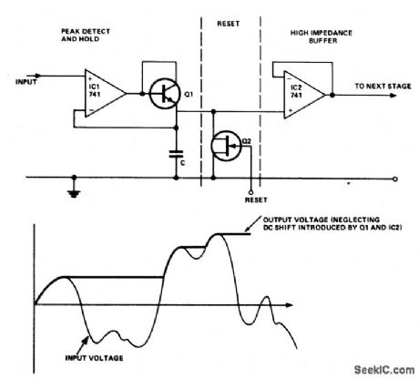
If the voltage at the input exceeds the voltage on the capacitor, then the output of the 741 goes positive, the diode conducts, and the capacitor is charged up to the input voltage-forward voltage drop of diode. When the voltage at the input is less than that on the capacitor, the output of the 741 goes negative, and the diode cuts off. To prevent the capacitor from discharging through the input resistance of the next stage, a high input impedance buffer stage (IC2) is used. The circuit can be reset by means of a FET or similar high impedance device connected across the capacitor. (View)
View full Circuit Diagram | Comments | Reading(1033)
Four_14_bit_outputs_from_one_DAC
Published:2009/7/24 11:23:00 Author:Jessie
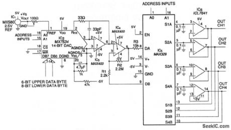
In this circuit, the low-leakage performance of a MAX329 provides an economical way to create four 14-bit DAC outputs from only one 14-bit DAC. Four 0.1-μF capacitors and an ICL7641 quad op amp sample the DAC voltage that is presented by the MUX. The A-section of the MAX329 scans the hold capacitors, while the B section closes a feedback loop, which connects the appropriate buffer within IC6 to a precision op amp (IC4). This loop effectively removes the buffer offset voltage. If a typical MUX charge injection of the 4 pC and a typical leakage (plus op-amp bias) of 1 pA are assumed, the voltage stored on each capacitor drops no more than 1 bit (out of 214) over 2.5 seconds at 25℃ . Maxim, 1992, Appications and Product Highlights, p. 9-5. (View)
View full Circuit Diagram | Comments | Reading(641)
Voltage_output_DAC
Published:2009/7/24 11:19:00 Author:Jessie
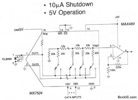
In this circuit, an MX7524 8-bit current output DAC is connected in an inverted configuration (voltage mode) by driving the IOUT pin with a 1.23-V reference (ICL8069). The DAC output drives a MAX480 where the gain is set so that full-scale output is 4 V. The power consumption is below 1 mW (operating) and much less shut down. The circuit operates when the On/Off input is at 5 V. When On/Off is at 0 V, supply current falls to 15μA, and the amplifier output falls to 0 V. The DAC input data can be retained if the WR input is used. Digital input lines must be driven with CMOS logic levels (rail-to-rail) to minimize supply current. Maxim, 1992,Appications and Product Highlights, p. 8-15. (View)
View full Circuit Diagram | Comments | Reading(952)
MOSQUITO_REPELLING_CIRCUIT
Published:2009/6/30 3:14:00 Author:May
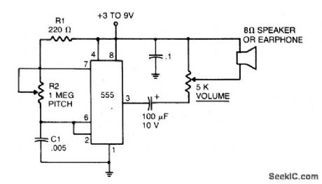
In the 555 oscillator circuit, adjusting R2 will provide output frequencies from below 200 Hz to above 62 kHz. Use a good quality miniature speaker so that it will produce frequencies on the order of 20 kHz. (View)
View full Circuit Diagram | Comments | Reading(846)
Square_root_circuit
Published:2009/7/24 11:09:00 Author:Jessie
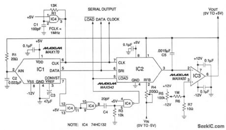
In this circuit, a 12-bit MAX543 DAC and a MAX170 A/D operate in the feedback loop of a single op amp to determine the square-root or a 0- to -5-V input signal. Both analog (VOUT) and digital outputs (serial DATA output) are provided. Accuracy surpasses 0.1% for -5-mV to 5-V inputs. The MAX543 squares the op-amp input, with an output that is proportional to IOUT=VREF(DAC code) +VIN. One DAC multiplying input is digital. The MAX170 A/D digitizes the op-amp output and transmits 12-bit data to the DAC. Consequently, the DAC VREF input and digital input carry the same value. The DAC output is then: IOUT=√5 ×√-VIN . Typical input/output examples are: VIN=-5.000 V, VOUT=+5.000 V; VIN=-0.5 mV, and VOUT=+50 mV. Maxim, 1992,Appications and Product Highlights, p. 8-14. (View)
View full Circuit Diagram | Comments | Reading(1477)
Fault_protected_8_channel_18_bit_dynamic_range_A_D_converter
Published:2009/7/24 10:54:00 Author:Jessie
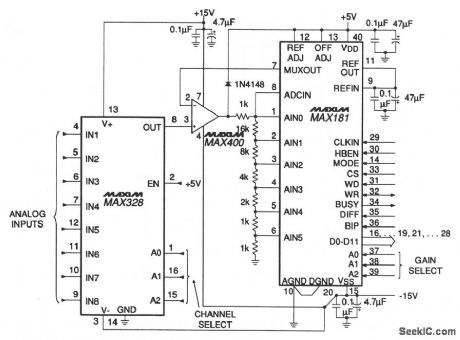
In this circuit, the MAX181 internal MUX forms a programmable-gain amplifier (PGA) with digitally-selected gains of 1, 2, 4, 8, 16, 32, 64, and 128. An external fault-protected MUX, the MAX378, selects from 8 input channels and protects the input for up to ±60-V voltage levels. Maxim, 1992, Appications and Product Highlights, p. 8-9. (View)
View full Circuit Diagram | Comments | Reading(614)
ULTRASONIC_BUG_CHASER
Published:2009/6/30 3:14:00 Author:May
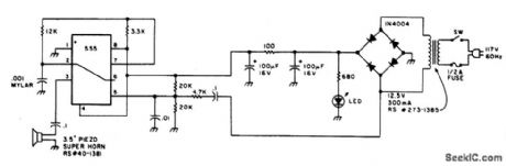
Low-intensity ultrasonic sound waves in the 30-45 kHz frequency band repel insects and small rodents. The unit is designed to generate a swept square wave from 30 to 45 kHz. The LM555 IC is wired as an ultrasonic oscillator driving a piezoelectric speaker of the hi-fi super-tweeter type. The output of the oscil-lator is swept by a 60-Hz signal from the ac input of the bridge rectifier. The LED acts as a pilot. (View)
View full Circuit Diagram | Comments | Reading(1003)
AC_HOT_WIRE_PROBE
Published:2009/6/30 3:13:00 Author:May
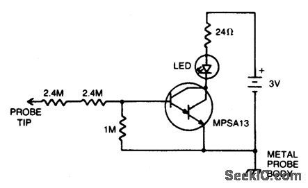
Insert the probe tip into either terminal of an ac outlet and hold the probe body against 3V anything that the circuit ground is connected to. The LED wi11 glow when the hot terminal is touched. Two 2.4 M resistors are used in the probe tip for safety (redundancy) reasons. (View)
View full Circuit Diagram | Comments | Reading(707)
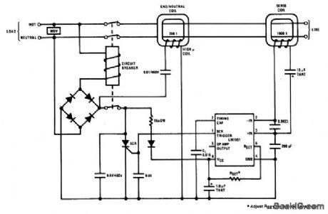
GROUND_FAULT_INTERRUPTER_120_Hz_NEUTRAL_TRANSFORMER_APPROACH
Published:2009/6/30 3:09:00 Author:May
View full Circuit Diagram | Comments | Reading(665)
| Pages:311/471 At 20301302303304305306307308309310311312313314315316317318319320Under 20 |
Circuit Categories
power supply circuit
Amplifier Circuit
Basic Circuit
LED and Light Circuit
Sensor Circuit
Signal Processing
Electrical Equipment Circuit
Control Circuit
Remote Control Circuit
A/D-D/A Converter Circuit
Audio Circuit
Measuring and Test Circuit
Communication Circuit
Computer-Related Circuit
555 Circuit
Automotive Circuit
Repairing Circuit