
Basic Circuit
Index 209
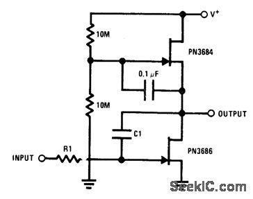
AC_COUPLED_JFET_
Published:2009/7/10 4:19:00 Author:May
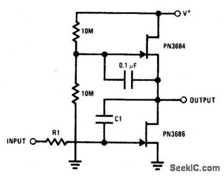
Use of C1 as Miller integrator or capacitance multiplier allows simple circuit to handle very long time constant while providing high voltage gain. Circuit also offers low distortion with low noise and high dynamic range.- FET Databook, National Semiconductor, Santa Clara, CA, 1977, p 6-26. (View)
View full Circuit Diagram | Comments | Reading(1058)
ADAPTER_FOR_COUNTER
Published:2009/7/10 4:17:00 Author:May
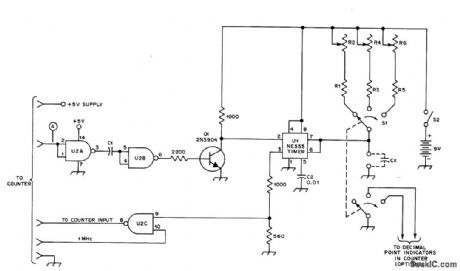
Converts counter into digital capacitance meter for measuring valuesclown to around 5 pF with better than 1% accuracy. Three ranges give full-scale values of 99,999 pF, 0,99999 μF, and 9.9999μF. Positive-going countenable command from frequency counter, applied to point A of gate U2A, removes short-circuit from unknown capacitor CX and enables gate U2C. Capacitor charges exponentially through R1 and R2 (range 1) to voltage at which threshold comparator at U1 makes flip4lop change state, shorting CX and disabling gate U2C. During charge time, 1-MHz pulses are applied to counter input. Counter reading then corresponds to capacitor value . C1 is 18 pF.R1 is 860K,R2 is 100K,R3 is 86K,R4 is 10K,R5 is 8.6K,R6 is 1K,and U2 is 7400 quad NAND gate.-R.F. Kramer,Using a Frequency Counteras a Capacitance Meter,QST. Aug 1977, p 19-22. (View)
View full Circuit Diagram | Comments | Reading(873)
SENSITIVE_CONTINUITY_CHECKER
Published:2009/7/10 4:14:00 Author:May
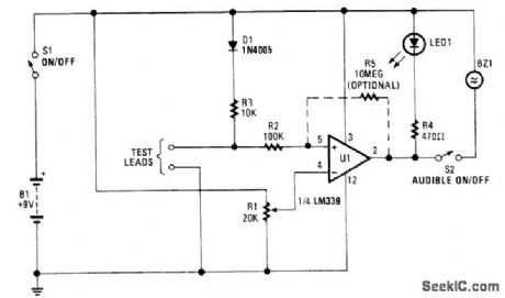
This continuity checker (built around an LM339 quad comparator with open-collector outputs) elimi-nates false readings because of coils or low-resistance devices in a circuit.
U1 is a comparator that acts as a sensing amplifier for the bridge circuit (R1 and D1, R3 and the unknown resistance, RX that is connected across the test leads. When RX is less than this predetermined value (by the setting of R1), the LED lights and BZ1 sounds. (View)
View full Circuit Diagram | Comments | Reading(754)
SQUARE_WAVE_ASTABLE_CIRCUIT
Published:2009/7/10 4:12:00 Author:May
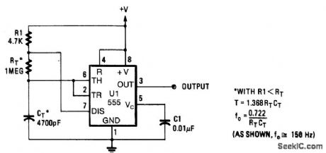
This 555 circuit produces a square wave. The frequency depends on the values of RT and CT, as per the design equations. (View)
View full Circuit Diagram | Comments | Reading(621)
JFET_WITH_AC_COUPLING
Published:2009/7/10 4:11:00 Author:May
Connection shown gives very high voltage gain. Use of C1 as Miller integrator or capacitance multiplier allows simple circuit to handle very long time constant.- FET Databook, National Semiconductor, Santa Clara, CA, 1977, p 6-26-6-36. (View)
View full Circuit Diagram | Comments | Reading(810)
TUNNEL_DIODE_COINCIDENCE_CIRCUIT
Published:2009/7/19 21:35:00 Author:Jessie
Determines coincidence of pulses from scintillation counter within nanosecond limits, for high-energy physics experiments. Circuit has limited timing jitter, good temperature stability, and is insensitive to transistor parameters.-C. Infante and F. Pandarese, Tunnel Diodes Stabilize Coincidence Circuits, Electronics, 34:46, p 133-135. (View)
View full Circuit Diagram | Comments | Reading(1155)
STORING_INTEGATOR_OUTPUT
Published:2009/7/10 4:07:00 Author:May
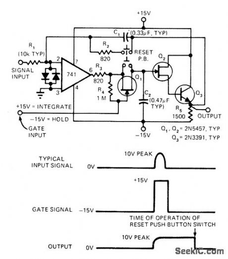
Modifiedsample-and-hold circuit with capacitive feed-back combines integrate,sample,and holdfunctions,fotuse In temporarily storing output of integrator Integrating amplifieris 741 opamp; for critical applications,FET opamp is preferable.-E. crovella, Circuit Combines Integrate,Sample and Hold Functions,EDN Magazine,Oct,20,1974, p 90. (View)
View full Circuit Diagram | Comments | Reading(769)
5_RANGE_LINEAR_SCALE_OHMMETER
Published:2009/7/10 4:02:00 Author:May
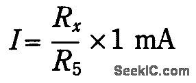
Rx is inserted h the feedback path of IC1.A known reference current is selected from reference voltage generator Q1,D1,and R5 through R9.A meter reading will be produced:
where R5=R5 through R9,as selected.This corresponds linearly to the value of Rx. (View)
View full Circuit Diagram | Comments | Reading(1000)
ELIMINATING_RINGING
Published:2009/7/10 4:01:00 Author:May
High-Q bandpass integrator reduces ringing significantly by amplifying AC input signal in two broadband differential amplifier stages, A1 and A2 before differentiation and selection by D1 and D2. Input gate pulse P1 and differentiated pulses drive AND logic that generates output pulse Ps coincident with zero crgssings of AC input. Leading edge of Ps will always occur at first zero crossing after P1 initiates gating action. If output drives balanced diode bridge, gating pedestal and AC signal transient are eliminated; high-Q bandpass integrator then has fast settling time, permitting faster repetition rates.-R. J. Tumer, Reduce Integrator Transients with Synchronized Gate Signals, EDN/EEE Magazine, Jan. 15, 1972, p 46-47. (View)
View full Circuit Diagram | Comments | Reading(1138)
DIRECT_READING_FIVE_RANGE
Published:2009/7/10 3:58:00 Author:May
Covers 1 pF to 1μF in five ranges, using easily available com ponents. Trigger source is free-running pulse generator using programmable UJT al and inverter-amplifier Q2 to produce narrow -12 V output pulse at constant frequency of about 500 Hz. For trigger pulse, NE555V timer connected as mono MVBR initiates output pulse whose width increases with value of capacitor under test. Meter reads average value of pulse wave form and may be calibrated directly to read capacitance. Range resistors should be 5% or better. 10K trimpot in series with meter serves for initial calibration. Zero-adjustment pot is needed only for lower ranges. Use zener-regu-Iated supply to provide 12 V at up to 50 mA. Full type number of al is A7T6028; 2N6027, 2N6028 2N6118, and HEP S9001 are similar. Single 0.0025-μF capacitor can be substituted for two 0.005-μF units in series.-C. Hall, Direct-Reading Capacitance Meter, Ham Radio, April 1975, p32-35. (View)
View full Circuit Diagram | Comments | Reading(772)
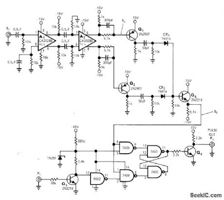
FALLOUT_TIME_OF_ARRIVAL_INDICATOR
Published:2009/7/19 21:29:00 Author:Jessie
Auto dock operates until fallout at level above 2 milliroentgens per hour arrives. Geiger-counter detection circuit then blows power-supply fuse, stopping clock with hands pointing to time of arrival.-R. W. Farmer and O. Reiner, Jr., Determining Arrival Time of Radioactive Fallout, Electronics, 31:31, p 69-71. (View)
View full Circuit Diagram | Comments | Reading(750)
DIGITAL_WITH_100_1_RANGE
Published:2009/7/10 3:56:00 Author:May
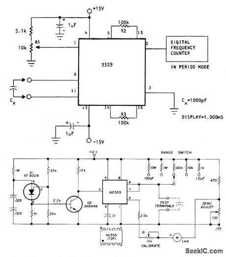
Frequency counter operated in period mode serves as readout for Optical Electronics 3329 voltage-to-frequency converter. Unknown capacitance is connected as external timing capacitance for IC, so output period of IC is directly proportional to unknown capacitance. To calibrate, conned known C and adjust R1 for correct reading on digital frequency counter. With values shown, 1 nF gives period of 1 ms.- Low Cost Capacitance Measurement, Optical Electronics, Tucson, AZ, Application Tip 10262. (View)
View full Circuit Diagram | Comments | Reading(780)
FAST_RECOVERY_
Published:2009/7/10 3:55:00 Author:May
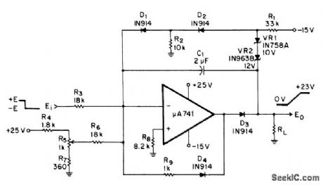
Two diodes and two zeners clamp output of integrator below saturation level of opamp, making recovery time approximately equal to slew rate. With values shown, integration time constant R3 C1 is 35.6 ms and output is clamped at +23 V. Output linearity is ±1%, and threshold range of circuit is -3 V to -10 V.-K. S. Wong, Fast-Recovery Integrator with Adjustable Threshold,EEE Magazine, Aug, 1970, p77. (View)
View full Circuit Diagram | Comments | Reading(735)
PHOTO_RELAY_USES_SR_90_SOURCE
Published:2009/7/19 21:27:00 Author:Jessie
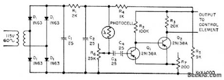
Interruption of high-energy beam from strontium-90 radioactive source changes resistance of cadmium sulphide photocell. Transistor amplifier converts variation into signal that actuates relay or other control element Source-detector separation must be less than 4 inches. Maximum counting rate is five pieces per second.-P. Weisman and S, L. Ruby, Solid-State Photocell Sees Through Haze, Electronics, 31:25, p 62-63. (View)
View full Circuit Diagram | Comments | Reading(731)
SLAVE_FLASH_TRIGGER
Published:2009/7/10 3:54:00 Author:May

The SCR is wired across the trigger circuit of the flash gun. Normally, the SCR is off, so the flash gun is able to charge to its trigger voltage. Photo transistor Q1 is used to monitor the light level.When a high-intensity flash occurs, Q1 briefly con-ducts and supplies gate current to the SCR. That causes the SCR to turn on, which then triggers the slave flash gun via the hot-shoe adapter terminals.
0nce the flash gun has triggered, the SCR's quickly tums off again. That happens because the current in circuit quickly falls below the SCR's hold-ing current. The resistor at the base of Q1 (R1)determines the sensitivity of the circuit. If you wish, you can reduce the sensitivity, simply by reducing the value of the resistor from that shown.The 1-kΩ resistor between the gate and cathode of the SCR (R3) prevents the SCR from false trigger-ing if high voltages are applied between the anode and the cathode. Q1 can also be a GEL14G2. (View)
View full Circuit Diagram | Comments | Reading(2393)
HIGH_INPUT_IMPEDANCE
Published:2009/7/10 3:50:00 Author:May

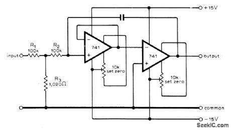
Two-opamp conoutput nection shown gives input resistance of 200 megohms and drift time of 90 min for0 to 10 V.-N. G. Boreham, Op-Amp Integrator, Wireless World, March 1977, p 42. (View)
View full Circuit Diagram | Comments | Reading(3781)
SLIDE_PROJECTOR_AUTO_ADVANCE
Published:2009/7/10 3:47:00 Author:May
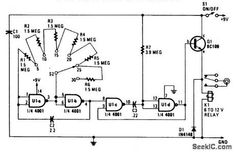
A 4001 CMOS Quad NORgate is set up as an astable multivibrator, which drives a simple differentia-tor and relay driver. Depending on the setting of S2, a delay of 5 to 30 seconds is generated. S2 and R1 through R6 can be replaced by a single 10-MΩ pot, if desired. (View)
View full Circuit Diagram | Comments | Reading(981)
CAMERA_TRIP_CIRCUIT
Published:2009/7/10 3:44:00 Author:May
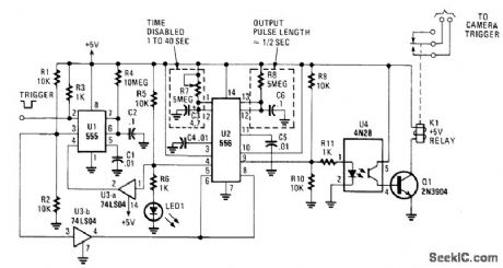
This circuit was used to trip a camera shutter. Grounding pin 2 of U1 makes pin 4 of U1 go high. This triggers both timers of dual timer U1. One output holds reset (pin 4) of U1 low to keep U1 from accepting another trigger, depending on the time constant of R7 and C3. This prevents camera film waste. The other timer is used to generate a 1/2-second pulse to drive U4 and Q1, the relay driver. K1 triggers the camera. (View)
View full Circuit Diagram | Comments | Reading(681)
INTEGATE_AND_DUMP
Published:2009/7/10 3:41:00 Author:May
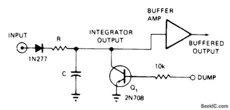
Transistor is used as switch, without power supply. Simple RC integrator will dump (discharge C) completely in about 1 μs when dump input is logic 1 (+5 V).Values of R and C determine time constant of integrator. Without power supply, circuh can only drive high-impedance load; for low-impedance load, add FET-input opamp such as Analog Devices 40J as buffer.-R. Riordan, Integrate and Dump Circuit Uses No Power Supply, EDN Magazine, Feb. 20, 1973, p 93. (View)
View full Circuit Diagram | Comments | Reading(2950)
CONTINUITY_CHECKER
Published:2009/7/10 3:41:00 Author:May
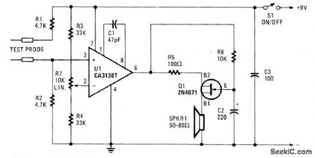
U1 is an op amp used as a comparator. When the test probes are shorted together, resistors R1 and R2 bias the noninverting input to half the supply voltage. The inverting input is biased by a voltage divider that consists of R3, R7, and R4. Resistor R7 is adjusted so that the voltage to the inverting input is lower than that to the noninverting input when the probes are shorted together. With continuity across the probes, U1's output goes high and supplies power to Q1, which is configured as arelaxation oscillator. The output of Q1 is fed to a high-impedance loudspeaker for an audio tone. When the probe is open, the nonin-verting input goes to the negative supply rail via R2. This action forces U1 is output low, which results in no output from the oscillator. (View)
View full Circuit Diagram | Comments | Reading(2419)
| Pages:209/471 At 20201202203204205206207208209210211212213214215216217218219220Under 20 |
Circuit Categories
power supply circuit
Amplifier Circuit
Basic Circuit
LED and Light Circuit
Sensor Circuit
Signal Processing
Electrical Equipment Circuit
Control Circuit
Remote Control Circuit
A/D-D/A Converter Circuit
Audio Circuit
Measuring and Test Circuit
Communication Circuit
Computer-Related Circuit
555 Circuit
Automotive Circuit
Repairing Circuit