
Switch Control
Index 10
SWITCH_CLOSURE_COU_NTER
Published:2009/6/29 2:40:00 Author:May
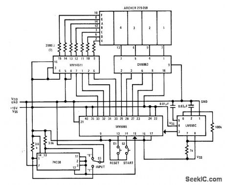
National MM5865 universal timer and counter chip is used with 74C00 debouncer and LM555C timer to drive digital display that counts closures of manual switch S3. Reset transition restores display to 0000. BCD segment outputs of MM5865 feed LED 4-digit display through MM14511 interface, whiledigit enable outputs go to display through DM8863 driver.— MOS/LSI Databook, National Semiconductor, Santa Clara, CA, 1977, p 2-23-2-32. (View)
View full Circuit Diagram | Comments | Reading(846)
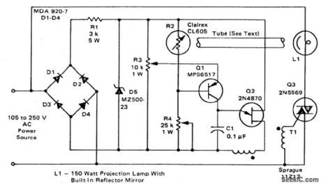
SCR automatic delay light switch circuit diagram
Published:2011/8/1 1:54:00 Author:Ecco | Keyword: SCR , automatic delay , light switch
SCR automatic delay light switch
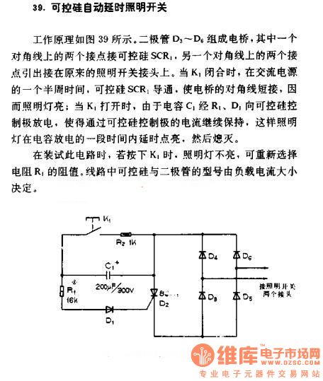
Working principle is shown in Figure 39. The diode D1 ~ D6 make up bridge, the two contacts on one of the diagonalis connected to SCR1, andthe other two contacts on the diagonal leads are connecting to the original light switch. When K1 is closed, in a half week time of AC power, SCR1 turns on, so that the diagonal of the bridge short connected, so lights are bright; when K1 is open, the capacitor C1 discharges through R1, D1 to the SCR system-level, making the current of SCR system-level maintain. So light is turned on in the capacitor discharging delayedtime, then turned off.
When peopleinstall this circuit, if pressing K1, lights off, you can re-select the resistance of resistor R1. The model of SCR and diode circuit determined by the size of the load current. (View)
View full Circuit Diagram | Comments | Reading(1480)
CURRENT_CONTROL_FOR_POWER_SWlTCH
Published:2009/6/29 2:15:00 Author:May
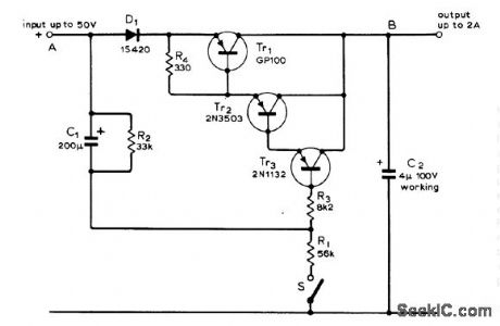
Circuit makes power supply current increase gradually from zero when supply is tumed on, to eliminate transients that sometimes cause alarming loudspeaker thumps in audio systems. Current through silicon power diode D1 is controlled by voltage on C1, which charges up after closing of switch with time constant C1R2R3/(R1 + R2). When switch is opened, rundown of supply curent is controlled by discharge of C1 through R2. Article also covers use of two current control circuits in tandem for handling higher Ioads.-P. J. Briody, Power Supply Delayed Switching, Wireless World, March 1975, p 139-141. (View)
View full Circuit Diagram | Comments | Reading(1115)
FOUR_POSITION_MOTOR_SWITCH
Published:2009/6/26 2:25:00 Author:May
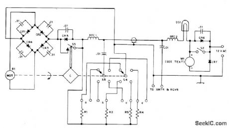
Single RF feed line also carries DC for 3-V permanent magnet DC motor B1 atop antenna tower, driving S3 and S4 for remote switching to antennas a, b, c, and d. Diagram shows switches set for feed to antenna a, with no drive applied to Bt since cam C has opened microswitch S5. CR5 and CR6 are now connected in series with opposite polarity, so neither positive nor negative halfwaves from 12-VAC supply can drive motor. If S2 is closed, poshive halfwaves start B1. Once started, motor runs until cam opens S5; if S2 has not yet been released, motor continues running on positive and negative halfwaves. Diode bridge CR1-CR4 makes motor rotate in only one direction for either drive polarity. If S2 is released, before S5 opens, motor stops. 6-V 1-A lamp DS1 comes on dimly when S2 is closed and brightens when S5 closes. If S2 is released now, B1 drives to next position and stops. If S2 is held down, switching continues. Meter M1 and CR7 identify position of switch. R1-R4 in range of 1K to 10K, are chosen to give 1/4, 1/2, 3/4, and full deflection of meter. Motor drives switch through 2860:1 reduction gears taken from alarm clock. All diodes are 50-PIV 1-A silicon such as 1N4001.-U.H.Lammers, A Remote Antenna Switch, QST,Aug.1974, p 41-43. (View)
View full Circuit Diagram | Comments | Reading(1027)
REMOTE_RING_EXTENDER_SWITCH
Published:2009/6/25 22:15:00 Author:May
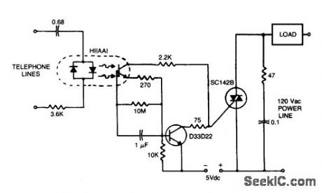


The circuit can operate lamps and buzzers from the 120V, 60 Hz power line while main-taining positive isolation between the tele-phone line and the power line. Use of the iso-lated tab triac simplifies heat sinking by removing the constraint of isolating the triac heat sink from the chassis. (View)
View full Circuit Diagram | Comments | Reading(785)
TWO_CHANNEL_SWITCH
Published:2009/6/25 21:56:00 Author:May
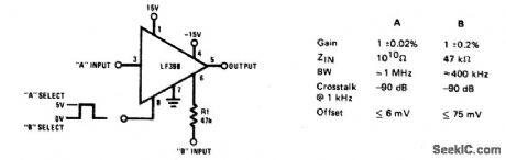
View full Circuit Diagram | Comments | Reading(712)
HIGH_FREQUENCY_SWITCH
Published:2009/6/25 21:53:00 Author:May

The 2N4391 provides a low ON resistance of 30 ohm and a high OFF impedance (<0.2 pF) when off. With proper layout and an ideal switch, the performance stated above can be readily achieved. (View)
View full Circuit Diagram | Comments | Reading(0)
DIFFERENTIAL_ANALOG_SWITCH
Published:2009/6/25 21:52:00 Author:May
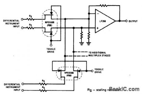
The NPD5566 monolithic dual is used in a differential multiplex application where Rd,coN) should be closely matched. Since Rd,coN) for the monolithic dual tracks at better than ±1% over wide temperature ranges (- 25℃ to +125℃), this makes it an unusual but ideal choice for an accurate multiplexer. This close tracking greatly reduces errors due to common-mode signals. (View)
View full Circuit Diagram | Comments | Reading(0)
SOUND_OPERATED_TWO_WAY_SWITCH
Published:2009/6/25 21:20:00 Author:May
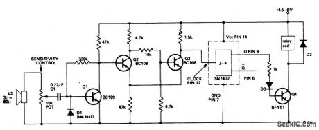
This circuit operates a relay each time a sound of sufficient intensity is made, thus one clap of the hands will switch it one way, a second clap will revert the circuit to the origi-nal condition. Q2 and Q3 form a Schmitt trigger. TheJK flip-flop is used as a bistable whose output changes state every time a pulse is applied to the clock input (pin 12). Q4 allows the output to drive a relay. (View)
View full Circuit Diagram | Comments | Reading(0)
COMPLEMENTARY_AC_POWER_SWITCHING
Published:2009/6/25 2:11:00 Author:May
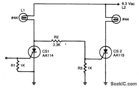
An input signal of less than 1 mA and 1 V is required to switch on CS1. As long as this input signal is maintained, CS1 will conduct during each positive half cycle of anode voltage, thereby energizing load L1 with half-wave rectified dc. L2 remains de-energized, since the anode of CS1 will not go more positive than 1.5 volts, and voltage divider R2 - R3 cannot provide enough voltage to trigger CS2. Upon removal of the input signal, CS1 will drop out.L1 will be de-energized, except for a small amount of ac current through R2 and R3. CS2will be triggered on at the beginning of each positive half-cycle, when CS1 anode voltage reaches 2 to 3 volts. CS2 will conduct for nearly the entire positive half-cycle energizing L2. It should be noted that the 6.3 volt lamps used will operate at 1/3 the rated brilliance because of the controlled switch half-wave rectifying action and will extend the operating lamp life by several orders of magnitude. Should full brilliance be desired, the anode supply voltage level should be raised to 9 volts ac. (View)
View full Circuit Diagram | Comments | Reading(0)
ZERO_POINT_SWITCH
Published:2009/6/25 2:01:00 Author:May
View full Circuit Diagram | Comments | Reading(1371)
PHOTOCELL_MEMORY_SWITCH_FOR_AC_POWER_CONTROL
Published:2009/6/24 23:42:00 Author:May
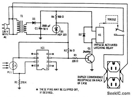
Provides remote control for ac-powered devices by using the beam of a flashlight as a magic wand. The important aspect of this gadget is that it remembers. Activate it once to apply power to a device and it stays on. Activate it a second time and power goes off and stays off. It consists of a combination of a high-sensitivity photocell, a highgain IC Schmitt trigger, and an impulse-actuated latching relay. (View)
View full Circuit Diagram | Comments | Reading(0)
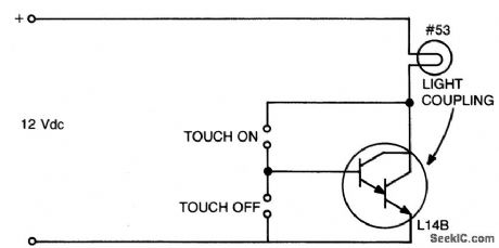
LATCHING,DOUBLE_BUTTON_TOUCH_SWITCH
Published:2009/6/24 23:11:00 Author:May
View full Circuit Diagram | Comments | Reading(0)
CMOS_TOUCH_SWITCH
Published:2009/6/24 23:10:00 Author:May
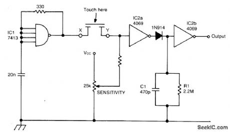
This touch switch does not rely on mains hum for switching. It can be used with battery powered circuits. Schmitt trigger IC1 forms a I 100 kHz oscillator and IC2a which is biased into the linear region, amplifies the output and charges C1 via the diode. IC2b acts as a level detector. When the sensor is touched, the os-cillator signal is severely attenuated which causes C1 to discharge and IC2b to change state. (View)
View full Circuit Diagram | Comments | Reading(0)
MOMENTARY_OPERATION_TOUCH_SWITCH
Published:2009/6/24 22:59:00 Author:May
View full Circuit Diagram | Comments | Reading(851)
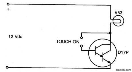
LOW_CURRENT_TOUCH_SWITCH
Published:2009/6/24 22:57:00 Author:May


Touching the on contacts with a finger brings pin 3 high, pair and supplying power to the load (transistor radio etc). transistor, and Q2 is chosen for the current required by the turning on the Darlington Q1 must be a high gain load circuit. (View)
View full Circuit Diagram | Comments | Reading(738)
TOUCH_SENSITIVE_SWITCH
Published:2009/6/24 22:56:00 Author:May
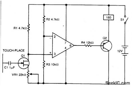
A high impedance input is provided by Q1, a general purpose field effect transistor. 741 op amp is used as a sensitive voltage level switch which in turn operates the current Q2, a medium current PNP bipolar transistor, thereby energizing the relay which can be used to control equipment, alarms, etc. (View)
View full Circuit Diagram | Comments | Reading(2028)
ADJUSTABLE_LIGHT_DETECTION_SWITCH
Published:2009/6/24 22:45:00 Author:May


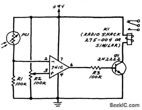
R2 sets the circuit's threshold. When the light intensity at PCI's surface is decreased, the resistance of PC1 a cadmium-sulfide photoresistor is increased. This decreases the voltage atthe inverting input of the 741. When the reference voltage atthe 741's noninverting input isproperly adjusted via R2, the comparator will switch from low to high when PC1 is darkened. This turns on Q1 which, in turn, pulls in relay K1. (View)
View full Circuit Diagram | Comments | Reading(1080)
VIDEO_SWITCH
Published:2009/6/24 21:48:00 Author:May
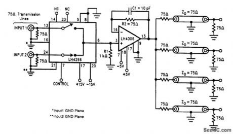
Using National Semiconductor LH4266 and LH4006, this circuit switches one of two inputs to four output (75Ω) lines. (View)
View full Circuit Diagram | Comments | Reading(1)
FREQUENCY_SWITCHER
Published:2009/6/24 21:32:00 Author:May
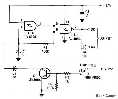
This transistor can achieve frequency switching in this CMOS astable oscillator. (View)
View full Circuit Diagram | Comments | Reading(0)
| Pages:10/15 123456789101112131415 |
Circuit Categories
power supply circuit
Amplifier Circuit
Basic Circuit
LED and Light Circuit
Sensor Circuit
Signal Processing
Electrical Equipment Circuit
Control Circuit
Remote Control Circuit
A/D-D/A Converter Circuit
Audio Circuit
Measuring and Test Circuit
Communication Circuit
Computer-Related Circuit
555 Circuit
Automotive Circuit
Repairing Circuit