
Switch Control
Index 3
_5_V_AT_3_A_SWITCHING
Published:2009/7/14 3:27:00 Author:May
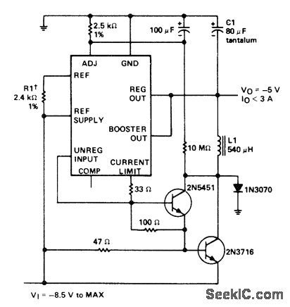
Negative-voltage regulator using SN52104 or SN72304 accepts input voltage range of -8.5 V to -40 V and pro-vides regulated output of -5 V with typical load regulation of 1 mV and input regulation of 0,06%. ICs are interchangeable with LM104 and LM304 respectively. L1 is 60 turns No. 20 on Arnold Engineering A930157-2 molybdenum permalloy core or equivalent.- The Linear and Interface Circuits Data Book for Design Engineers, Texas Instruments, Dallas, TX, 1973, p 5-5. (View)
View full Circuit Diagram | Comments | Reading(889)
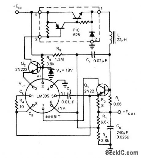
HIGH_VOLTAGE_POSITIVE_SWITCHING
Published:2009/7/14 3:24:00 Author:May
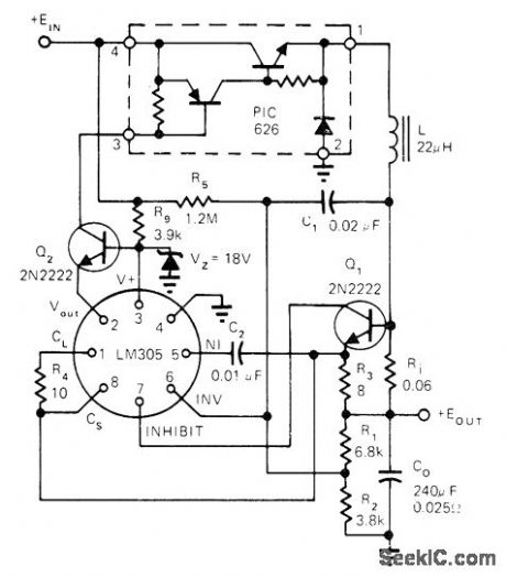
Uses 18-V zener in series with 3.9K resistor to provide power for LM305 IC regulator. Q2 provides base drive for PIC626 hybrid power switch and isolates output of LM305 from switch.-L. Dixon and R. Patel, Designers' Guide to: Switching Regulators, EDN Magazine, Oct. 20, 1974, p 53-59. (View)
View full Circuit Diagram | Comments | Reading(983)
_5_V_FLYBACK_SWITCHING
Published:2009/7/14 3:18:00 Author:May

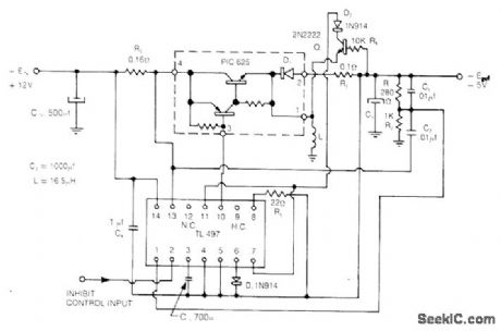
Uses Unitrode PIC625 regulator operating at 25 kHz and TL497 control circuit operating in current-limiting mode to give line and load regulation of 0.2% for input voltage of 12 V ±25%. Efficiency is 75%. Short-circuit current is automatically limited to 3 A.- Flyback and Boost Switching Regulator Design Guide, Unitrode, Watertown, MA, 1978, U-76, p 5. (View)
View full Circuit Diagram | Comments | Reading(2645)
VARIABLE_SWITCHING_FREQUENCY
Published:2009/7/14 3:12:00 Author:May

TL497 switching regulator operates at maximum frequency under maximum load conditions. For smaller loads, duty cycle is varied automatically by maintaining fixed ON time and varying switching frequency. Circuit optimizes efficiency at about 75% by reducing switching losses as load decreases.-J. Spencer, Monolithic Switching Regulators-They Fit Today's Power-Supply Needs, EDN Magazine, Sept. 5, 1977, p 117-121. (View)
View full Circuit Diagram | Comments | Reading(1954)
5_V_40_A_20_kHz_SWITCHED_MODE
Published:2009/7/14 3:11:00 Author:May
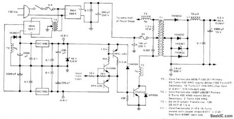
Uses Motorola 2N6544 power transistors operating with 3-A collector current (other half of power stage is identical). Bridge rectifier and capacitive filter connected directly to AC line form 150-VDC sup-ply for inverter operating at 20 kHz. Regulators MC7806 and MC7906 operating from MDA9221 bridge rectifier of 15-W filament transformer T3 provide ±6 V for logic circuits that provide pulse-width modulation for inverter. When logic signal is high, MPS-U51 saturates and supplies 1 A to base of 2N6544 inverter power transistor When logic is low, MPS-U95 Darlington holds inverter transistor off.-R. J. Haver, Switched Mode Power Supplies-Highlighting a 5-V, 40-A Inverter Design, Motorola, Phoenix, AZ, 1977, AN-737A, p 10. (View)
View full Circuit Diagram | Comments | Reading(1498)
5_V_FIXED_OFF_TIME_SWITCHING
Published:2009/7/14 2:53:00 Author:May
Uses LM305 regulator and Unitrode hybrid power switch in PIC600 series. Operates in fixed OFF-time mode. Output ripple of 100 mV P-P is independent of input voltage range of 20 to 40 V for output of +5 V ±1%. Switching speed is nominally 50 kHz but can go up to 100 kHz. Article covers theory of operation in detail.-L. Dixon and R. Patel, Designers' Guide to: Switching Regulators, EDN Magazine, Oct. 20, 1974, p 53-59. (View)
View full Circuit Diagram | Comments | Reading(765)
_5_V_SWITCHING_AT_10_A
Published:2009/7/14 2:52:00 Author:May
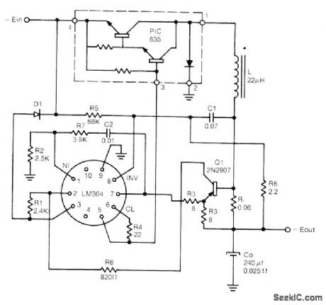
Uses Unitrode PIC635 hybrid power switch with LM304 regulator for switching speeds up to 100 kHz with input voltage range of 20-40 V. 01 provides cur-rent-limiting action.- Switching Regulator Design Guide, Unitrode, Watertown, MA, 1974, U-68A, p 9. (View)
View full Circuit Diagram | Comments | Reading(0)
5_24_V_SWITCHING
Published:2009/7/14 2:49:00 Author:May

Choice of regulator in μA7800 series determines fixed output voltage. Devices are available for rated outputs of 5, 6, 8, 12, 15, 18, and 24 V, positive or negative, with output current ratings of 100 mA, 500 mA, or 1 A. If input voltage is greater than maximum input rating of regulator used, add voltage-dropping zener Dl to bring voltage between pins 1 and 3 down to acceptable level.- Signetics Analog Data Manual, Signetics, Sunnyvale, CA, 1977, p 668, (View)
View full Circuit Diagram | Comments | Reading(872)
33_OR_5_V_ANALOG_SWITCHES
Published:2009/7/14 2:33:00 Author:May
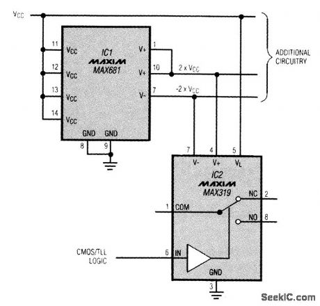
By adding a single component to a 3-V only or 5-V only board,you can operate conventional CMOS analog switches with Performance approaching that specified with ±15-V Supplies, This means fast switching,low ON resistance,CMOS /TTL compatibility, low power consumption,and a signal range (±Vcc) that exceeds the input supply range (Vcc to ground).Simply add a charge-ump voltage converter:(IC1),which produces±2-Vcc outputs from a Vcc input .These unregulated voltages ensure reliable switch operation for Vcc levels as low as 3 V. Logic thresholds for the switch remain unaffected A Vcc of 3 V (for instance)produces,±6 v rails for the switch (IC2),resulting in ON resistance<30Ω,switching times<200 ns,leakage<0.1 nA,and Vcc ourrent<0.5mA Raising Vcc to 5 V produces±10-V rails,resulting in ON resistance<20Ω,switching times<150 ns,leakage<0.4 nA,and Vcc current<l.3 mA IC1 can easily power additional switches and/or low-power Op amps,but more than a few milliamperes of load current degrades Performance by lowering the unregulated supply rails.
(View)
View full Circuit Diagram | Comments | Reading(884)
VOICE_ACTIVATED_TAPE_RECORDER_SWITCH
Published:2009/7/14 1:27:00 Author:May
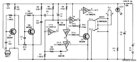
A schematic of the tape recorder switch is shown The circuit can be powered by B1, which is four AA batteries in series or any 6-Vdc supply. Audio signals from the electret Microphone,MIC1,are coupled via capacitor C1 to two audio-amplification stages centered around transistors Q1 and Q2 A 5000-Ω Potentiometer, R12,provides a sensitivity control that sets the audio level at which the switch will activate a tape recorder The audio input to the digital switching section of the circuit is biased at half the supply voltage by two 1-percent,1-MΩ,metal-film resistors (R6 and R7) Integrated Circuit U1 is a 74HC14 hex Schmitt-trigger inverter. With a 6-V power supply,the Schmitt inverter gates will have a l-V hysteresis gap between 2.2 and 3.2 V That means that the input to a Schmitt inverter must rise above 3.2V for the output to go low; but must fall below 2.2V for the output to return to a high,The low on pin 3 of U1-b in the Presence of audio is presented to pin 11 of U1-e and ends up at pin 8 of U1-d That will pull pin 1 low in the absence of an audio signal from the microphone,making pin 2 high Diode D2 blocks the discharging of C5 through its original charging path, so C5 starts to discharge through R9. After that delay, the voltage at pin 3 rises above 3.2 V, thus removing the connection from terminal A to ground and turning off the tape recorder. A continuous audio input to pin 1 will hold pin 4 high, but soon as it ceases, the time-out process begins. When power is applied to the circuit using switch S2, LED1 lights. However, if the ground connection to R11 is removed, and that end of the resistor is then connected to terminal X (pin 6 of U1-c), the LED will instead light only when the output of the circuit is active. (View)
View full Circuit Diagram | Comments | Reading(1680)
80_VRMS_ANALOG_SWITCH
Published:2009/7/14 1:07:00 Author:May
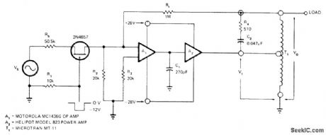
Developed for switching high-level analog signals with speed, accuracy, and reliability, for such applications as digital-to-synchro converters. Feedback net-work stabilizes output against changes in circuit parameters. For AC signal inputs between±10 V, -12 VDC on gate of FET blocks input channel and R2 grounds inverting input of opamp A1 to prevent noise pickup and minimize voltage offset. Grounding gate of FET turns on input channel;input signal is then amplified by A1 and fed to unity-gain power opamp A2.-D.J. Musto, Analog Switch and IC Amp Controls 80V RMS, EDN Magazine, Feb 20, 1973, p 91-92. (View)
View full Circuit Diagram | Comments | Reading(1022)
DUAL_FUNCTION_SWITCH
Published:2009/7/14 1:05:00 Author:May
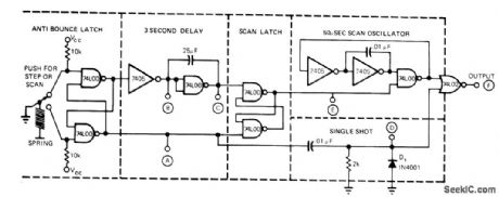
Pressing switch for less than 3 s produces single output pulse about 5μs wide. When switch is pressed longer than 3 s, single pulse is generated as before, and scan oscillator is turned on 3 s later. Oscillator runs as long as switch is held down, for producing repetitive stepping motion. Applications include positioning of test probes on single semiconductor chip or on wafer of several hundred chips, or indexing device either step by step or automatically through desired number of steps.-J. McDowell, Single Switch Controls Two Functions, EDN Magazine, April 5, 1974, p 78 and 80. (View)
View full Circuit Diagram | Comments | Reading(889)
SIGNAL_CONTROLLED_SWITCH
Published:2009/7/14 1:04:00 Author:May
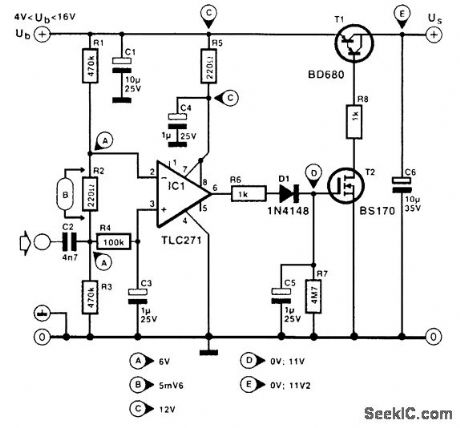
This signal-controlled switch actuates or deactuates AF equipment, including preamplifiers, power amplifiers, and filters. It is particularly useful for battery-operated equipment because, owing to the low current drain of 12 to 14μA, there is no need to switch the AF equipment off. When the switch has not detected any AF signal for 10 seconds, it switches off the supply to the equipment. (View)
View full Circuit Diagram | Comments | Reading(1218)
SYNCHRONIZED_SWITCHING
Published:2009/7/14 1:02:00 Author:May
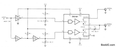
Transients occurring during switching between two amplifier channels are attenuated by synchronizing turn on of one switch in DG181 JFET analog switch with turnoff of other switch. Switching action is controlled by logic input,- Analog Switches and Their Applications, Siliconix, Santa Clara, CA, 1976, p 7-61. (View)
View full Circuit Diagram | Comments | Reading(831)
LOGIC_CONTROLLED_ANALOG_SWITCH
Published:2009/7/14 1:00:00 Author:May
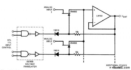
2N4860 JFETs were chosen for low leakage and 25-ohm ON resistance in switching circuit. LM102 opamp serves as voltage buffer. DS7800 IC provides switch drive under control of DTL or TTL levels.- FET Databook, National Semiconductor, Santa Clara, CA, 1977, p 6-26-6-36. (View)
View full Circuit Diagram | Comments | Reading(897)
DIAMOND_BRIDGE_ANALOG_SWITCH
Published:2009/7/14 0:55:00 Author:May
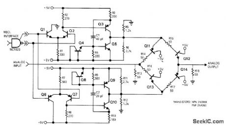
Analog signals up to 3 V P-P are switched in less than 3 ns to meet requirements of multiplexer and sample-and-hold portions of 100 Mb/s PCM telemetry encoder. Symmetrical drive circuits turn four-transistor diamond bridge on and off at 20-MHz clock frequency. Transient-coupled pullback transistors Q5 and Q9 speed turnoff. Typical rise time is 1,5 ns and fall time is 2 ns for 1-VDC analog input.-W. A. Vincent, Diamond Bridge Improves Analog Switching, EDN Magazine, Feb 15, 1971, p 41-42. (View)
View full Circuit Diagram | Comments | Reading(1617)
FET_ANALOG_SWITCH
Published:2009/7/14 0:51:00 Author:May
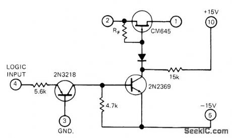
Simple level-shifting driver provides analog switching. Input of logic 1 makes emitter and collector current flow in input PNP transistor, for shifting from logic to -15 V. This current makes NPN transistor turn on so its collector is -15 V, diode is forward-biased, and FET gate is about -14.3 V. At logic 0, both transistors are off and driver output is at +15 V. Diode is now reverse-biased, turning FET on to provide desired switching action between outputs 1 and 2.-J. Cohen, Solid-State Signal Switching: Ifs Getting Better All the Time, EDN Magazine, Nov. 15, 1972, p 22-28. (View)
View full Circuit Diagram | Comments | Reading(2108)
FERRITE_CORE_SWITCHING
Published:2009/7/14 0:50:00 Author:May
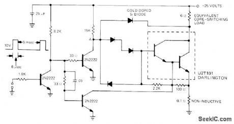
Darlington transistor driven by low-power current stage serves for saturating groups of ferrite cores in phased arrays for radar systems or in read/write core switching for memory systems. Circuit provides fast rise and fall times.- Designer's Guide to Power Darlingtons as Switching Devices, Unitrode, Watertown, MA, 1975, U-70, p 4. (View)
View full Circuit Diagram | Comments | Reading(984)
VIDEO_SWITCH
Published:2009/7/14 0:49:00 Author:May
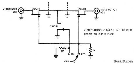
2N4391 FETs provide ON resistance of only 30 ohms and OFF impedance less than 0.2 pF, to give performance comparable to that of ideal high-frequency switch. Attenuation is greater than 80 dB at 100 MHz. Insertion loss is about 6 dB.- FET Databook, National Semiconductor, Santa Clara, CA, 1977, p 6-26-6-36. (View)
View full Circuit Diagram | Comments | Reading(0)
ANALOG_WITH_HIGH_TOGGLE_RATE
Published:2009/7/14 0:46:00 Author:May
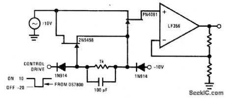
Simple commutator circuit provides low-impedance gate drive to PN4091 FET analog switch for both ON and OFF drive conditions. For high-frequency signal handling, circuit also approaches ideal gate drive conditions by providing low AC impedance for OFF drive and high AC impedance for ON drive.- FET Databook, National Semiconductor, Santa Clara, CA, 1977, p 6-26- 6-36. (View)
View full Circuit Diagram | Comments | Reading(827)
| Pages:3/15 123456789101112131415 |
Circuit Categories
power supply circuit
Amplifier Circuit
Basic Circuit
LED and Light Circuit
Sensor Circuit
Signal Processing
Electrical Equipment Circuit
Control Circuit
Remote Control Circuit
A/D-D/A Converter Circuit
Audio Circuit
Measuring and Test Circuit
Communication Circuit
Computer-Related Circuit
555 Circuit
Automotive Circuit
Repairing Circuit