
Switch Control
Index 6
ON_OFF_TOUCH_SWITCH
Published:2009/7/11 1:20:00 Author:May
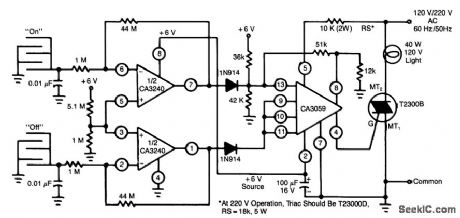
This circuit uses a CA3240 dual BiMOS op amp to sense small currents flowing between the contact points on a touch plate. The high input impedance of the CA3240 allows the use of 1-MΩ resistors in series with the touch plates to ensure user safety. A positive output on either pin 7 (ON) or pin 1 (OFF) of the CA3240 actuates the CA3059 zero-voltage switch, which then latches the triac on or turns it off. The internal power supply of the CA3059 powers the CA3240. (View)
View full Circuit Diagram | Comments | Reading(0)
TOUCH_SWITCH_Ⅰ
Published:2009/7/11 1:18:00 Author:May
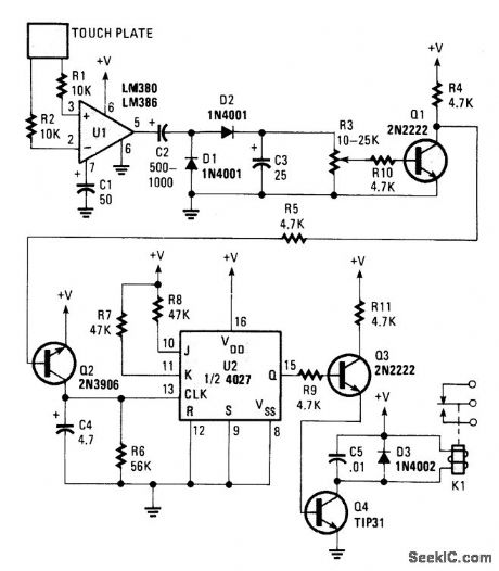
This switch reacts to the touch of a finger to turn lights and/or appliances on or off. The device uses the human body as an antenna to pick up 60-Hz hum, which is applied to a metal plate by your finger. The signal is fed to the input of U1, an LM380 audio-power amplifier. An LM386 should work as well.The 60-Hz output from the amplifier is rectified by D1 and D2, then filtered by C3. Potentiometer R3 sets the trigger voltage used to saturate Q1. When Q1 turns on, the collector end of R4 goes almost to ground and provides the needed voltage to turn on Q2. Transistor Q2 turns on and clocks. The flip-flop is configured for toggle-mode operation, so its output switches states with each clock pulse.The 4027 (U2) is wired to toggle by tying the J and K inputs high and the set and resets low. Transis-tor Q3 is connected to the Ooutput through the 4.7-kΩ resistor. Transistor Q3 drives Q4, the relay driver. Be sure that the load does not exceed the relay ratings. (View)
View full Circuit Diagram | Comments | Reading(1067)
OVER_TEMPERATURE_SWITCH
Published:2009/7/11 0:32:00 Author:May

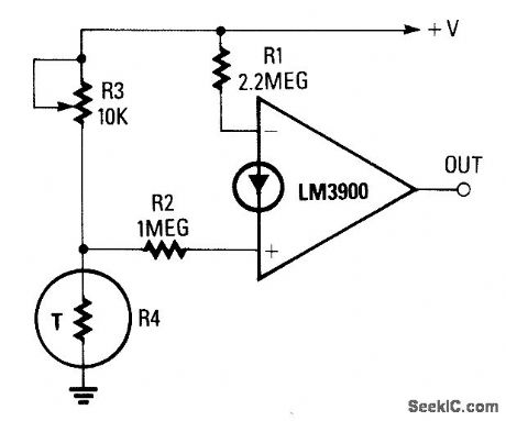
The output goes high when a preset tempera-ture is exceeded. A fixed half-supply reference voltage feeds a reference current to the inverting input, and a variable current is fed to the noninvert-ing input. Resistor R6 is a negative-temperature-coefficient (NTC) thermistor, so the potential at the junction of R5 and R6 rises with temperature. The op amp will switch high when that voltage exceeds the half-supply value. The trip temperature can be preset via R5. (View)
View full Circuit Diagram | Comments | Reading(1012)
UNDER_TEMPERATURE_SWITCH
Published:2009/7/11 0:30:00 Author:May
The reference current is fed from the supply voltage via R1, to the inverting terminal, and the variable (noninverting) current is supplied from the junction of R3 and R4. Because the value ofR1 is approximately double that of R2, and generates a current that is proportional to the supply voltage, the trip temperature (preset via R3) is independent of the supply voltage. (View)
View full Circuit Diagram | Comments | Reading(881)
SIGNAL_SWITCHER
Published:2009/7/10 22:40:00 Author:May
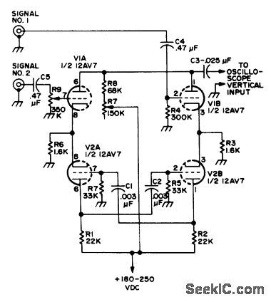
Two-tube electronic switch serves in effect to provide simultaneous presentation of two different signals on CRO screen by switching signals alternately to vertical input at rate fast enough so both displays are seen.-Novice Q & A, 73 Magazine, March 1977, p 187. (View)
View full Circuit Diagram | Comments | Reading(723)
BOUNCE_FREE_AUTO_REPEAT_SWITCH
Published:2009/7/10 21:17:00 Author:May
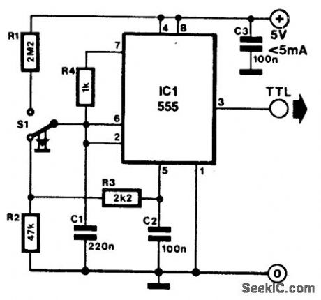
This switch that keeps pulsing as long as it is pressed is often required. The circuit here used the well known Type 555 for this purpose. Its output is a TTL-compatible signal. Pin 5 of the timer has a potential of 67% of the supply voltage, UCC In the quiescent condition (switch not pressed), C1 charges via R2 and R3 to a voltage that is lower than that at pin 5, and thus is also lower than the toggle voltage.When the switch is pressed, C1 is rapidly charged via R1 to the toggle voltage, upon which the timer emits a pulse. At the same time, the capacitor is discharged again via R4. As long as the switch is pressed, the circuit functions as an astable toggle and produces pulses. When it is released, the capacitor cannot charge to the toggle voltage. (View)
View full Circuit Diagram | Comments | Reading(834)
SWITCHING_CIRCUIT
Published:2009/7/10 20:57:00 Author:May

This switching circuit acts like a bank of interlocked mechanical switches; pushing one of the buttons latches its corresponding output and unlatches a previously selected output. A pair of inverters forms a latch for each output.Pressing button B1, for example, applies a positive pulse, via resistor diode D1B, to the input of the first output's, 0UT1, latch. This positive pulse will set OUT1 high. Feedback locks OUT1's pair of converters in this HIGH state. Meanwhile, the pulse will also pass through diode D1A to the differentiator that is formed by C and R2. The differentiator will shorten the pulse.The shortened pulse goes to all the latches and resets all of them, except the latch that sees the longer setting pulse. Obviously, if you press more than one button at once, more than one output will latch at once. (View)
View full Circuit Diagram | Comments | Reading(1268)
ON_OFF_SWITCH
Published:2009/7/10 20:54:00 Author:May
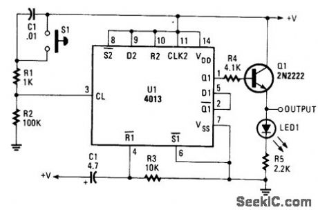
A CD 4013 dual-D flip-flop is used to drive an emitter-follower. This circuit can be used where a simple pushbutton on/off is desired. (View)
View full Circuit Diagram | Comments | Reading(7595)
SATELLITE_TV_AUDIO_SWITCHER
Published:2009/7/10 20:52:00 Author:May
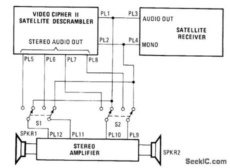
Some channels offer a separate audio mode (SAP) in a second language. It is usually transmitted on 6.8 MHz, which is the frequency used for unscrambled channels. The audio in the scrambled channels is transmitted along with the picture, so when the descrambler descrambles the signal, it also descrambles the audio in stereo. When the channel offers SAP, you'll find it on 6.8 MHz.The switches are a pair of DPDT switches that have the toggle handles tied together. In one position, you hear the audio in stereo and in the other position, you hear the SAP. Just turn down the volume level on the TV and you can connect it to a stereo amplifier and a pair of speakers. (View)
View full Circuit Diagram | Comments | Reading(776)
DIODE_RF_SWITCH
Published:2009/7/10 20:47:00 Author:May
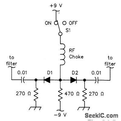
D1 and D2 can be IN914B- or HP2800-senesdiodes(for UHF).The loss is over 60 dB h the OFF state,and less than 3 dB at 3.5 to 30 MHz(using common IN914B diodes). (View)
View full Circuit Diagram | Comments | Reading(872)
PRECISION_NARROW_BAND_TONE_SWITCH
Published:2009/7/10 20:43:00 Author:May
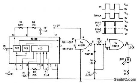
This signal tracker and lock detector combine to make a precision tone switch. Filter R3/R4/C2 determines signal capture and tracking range, as well as settling time.. Max. VCO frequency: R1C1. Min. VCO frequency: (R1+R2)C2Pin 9 voltage affects both. The minimum at pin 9 is 0 V and the maximum at pin 9 is VDD. In the lock detector, the PC (phase comparator) outputs are pulses whose width is proportional to the phase difference between the two PC inputs. At lock up, the two PC outputs are almost mirror images. The output of IC1A remains low and IC1B is high. This lights LED1. If the loop is unlocked, the LED will not light. (View)
View full Circuit Diagram | Comments | Reading(760)
N+1WIRES_CONNECT_N_HALL_EFFECT_SWITCHES
Published:2009/7/10 5:03:00 Author:May
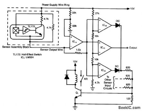
Hall-effect switches have several advantages over mechanically and optically coupled switches. Their major drawback is that they require three wires per device. This circuit, however, reduces this wire count to N + 1 wires for N devices.Amplifter IC1A is configured as a current-to-voltage converter. It senses the sensor assembly's output current. When the Hall-effect switch is actuated, the sensor's output current increases to twice its quiescent value. Amplifter IC1B, conftgured as a comparator, detects this increase. The comparator's output goes low when the Hall-effect switch turns on.The circuit also contains a fault-detection function. If any sensor output wire is open, its corresponding LED will turn on. If the power-supply line opens, several LEDs will tum on. A short circuit will also tum an LED on. Every time an LED tums on, Q1 turns on and the alarm relay is actuated.
(View)
View full Circuit Diagram | Comments | Reading(722)
POWER_MOSFET_SWITCH
Published:2009/7/10 4:15:00 Author:May

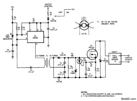
This solid-state switch senses and interrupts an overcurrent condition within 2μs. I1 allows the circuit to float. IC1 runs at 150 kHz and full-wave doubler D1/D2 provides 15 V to the gate of Q1. An overcurrent sensed across R1 triggers Q3, removes gate bias from Q1, and opens the circuit formed by the full-wave bridge and Q1. C1 and R3 allow the circuit to handle surges.
(View)
View full Circuit Diagram | Comments | Reading(1571)
5_VSUPPLY_HIGH_SIDE_SWITCHER
Published:2009/7/10 4:07:00 Author:May
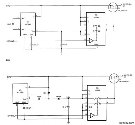
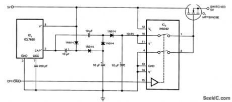
Requiring only 10 uA of quiescent current, the circuit of (Fig. 62-1(a)) produces only 0.1-Ω ON-resis-tance. IC1 is a charge pump voltage converter to produce a -5-V level, so analog switch IC2 can provide a 10-V swing to MOSFET Q1.
This circuit uses a voltage converter to enable the analog switch to apply a 4.3-V swing to logic level NMOS power transistor Q1. ON resistance is 0.03 Ω typical.
This circuit uses additional stages in the voltage-multiplying circuit to provide a higher gate voltage swing. This would enable the use of a convener for an NMOS switching transistor. (View)
View full Circuit Diagram | Comments | Reading(772)
FAST_DUMP_SWITCH_
Published:2009/7/10 3:46:00 Author:May


Requires only 350 ns to dump 6-V output to level of 3 mV. Transistors are connected so one of them is biased in forward mode independently of output polarity. Both transistors tum on during dump interval.Transistor operating in forward mode determines initial discharge rate until it saturates, after which inverted-mode transistorcontinuesto discharge capacitor. Offset voltage error is only -25 μV. Opamp is Analog Devices 120 or equivalent having unityqain bandwidth above 100 MHz and slew rate above 200 V/us.-F. Tarico, Fast Bipolar Dump Switch Has Low Offset, EDN Magazine,Nov5,1974.p 66. (View)
View full Circuit Diagram | Comments | Reading(780)
MICROPHONE_CONTROLLED_VOICEACTIVATED_SWITCH
Published:2009/7/10 3:31:00 Author:May
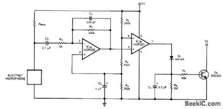
An electret microphone feeds a bandpass ftlter circuit (IC1A), then feeds a comparator, which in turn drives Q1. Q1 is a switch that conducts when audio from IC1B causes D1. C4. R6. and R7 to bias it oN. (View)
View full Circuit Diagram | Comments | Reading(840)
ONE_MOSPOWER_FET_ANALOG_SWITCH
Published:2009/7/10 3:26:00 Author:May
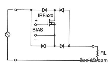
Using four diode in an array allows using only one MOSPOWER transistor for analog switching.The current flow is controlled by keeping the source-base connection of the MOSFET towards the load. Be sure to use diodes capable of handling the load current and a transistor whose breakdown voltage specification exceeds the peak analog voltage anticipated. Operationally, by increasing the gate-to-source bias voltage, the MOSFET turns on. For applications other than either full-on or full-off, care must be taken not to exceed the dissipation of the MOSPOWER transistor. A suitable heatsink cannot be overstressed in such applications. (View)
View full Circuit Diagram | Comments | Reading(914)
RF_POWER_SWITCH
Published:2009/7/10 3:20:00 Author:May
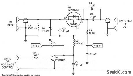
This rf power switch operates at 1.7 MHz with a 50-V Source and load.Its on loss is 0.2 dB and its off isolation is 30 dB.It provides 40-W PEP,45 VPEAK and 0.9 APEAK. The control input can come from CMOS ,TTL,LS,etc.,to turn on Q1,which turns on Q2,a TMOS MTP3N35. (View)
View full Circuit Diagram | Comments | Reading(945)
SOUND_ACTIVATED_SWITCH
Published:2009/7/10 3:08:00 Author:May
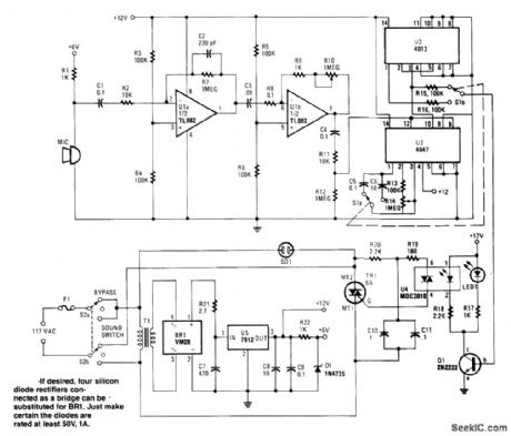
This circuit provides either latched switching or timed switching.U1A and U1B provide audio ampliftcation from the microphone,U2 is a retriggerable monostable multivibrator. S1A and S1B select either U3,a flip-flop,or U2. R13 and R14 allow a 6- to 60-second timer delay after the sound ceases,in the timed mode。BR1,U5,and associated components form a power supply.Q1 drives optocoupler U4 andtriggers triac TR1. (View)
View full Circuit Diagram | Comments | Reading(0)
VOICE_OPERATED_SWITCH
Published:2009/7/10 2:31:00 Author:May
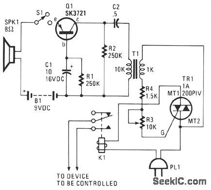
The sound picked up by SPKR1, which acts as a microphone, is fed to transistor amplifier Q1. The output of Q1 is applied across coupling transformer T1 and is used to drive the gate circuit of Triac TR1. TR1 is used to lend a latching effect to the action of the relay. (View)
View full Circuit Diagram | Comments | Reading(120)
| Pages:6/15 123456789101112131415 |
Circuit Categories
power supply circuit
Amplifier Circuit
Basic Circuit
LED and Light Circuit
Sensor Circuit
Signal Processing
Electrical Equipment Circuit
Control Circuit
Remote Control Circuit
A/D-D/A Converter Circuit
Audio Circuit
Measuring and Test Circuit
Communication Circuit
Computer-Related Circuit
555 Circuit
Automotive Circuit
Repairing Circuit