
Switch Control
Index 7
SOUNG_ACTIVATED_SWITCH
Published:2009/7/10 2:30:00 Author:May
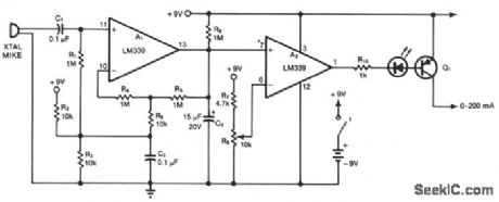


A1 and A2 are two sections of a quad comparator. The first, A1, functions as an amplifier and detector. Resistors R5 and R6 set the gain at 100; the output of A1 is an open collector to negative-peak-rectify the output with a decay time constant determined by R9 and C3. This dc output is then compared with the reference level selected by R8. A2 triggers switch Q1, and an LED inserted in the base drive of Q1 gives visual indication of switch closure. The standby battery drain is 2 mA. Use potentiometer R8 to select the desired sensitivity. (View)
View full Circuit Diagram | Comments | Reading(1015)
FAULT_SENSING_SWITCH
Published:2009/7/9 23:19:00 Author:May
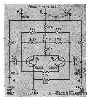
When fault in microwave system has effect of closing switch 3, gated delcty shortens output pulse for that function when binary input signals are negative.-J. B. Bullock, Pulse-Coded Fault Alarm in Microwave Systems, Electronics, 33:1, p 82-84. (View)
View full Circuit Diagram | Comments | Reading(808)
FLIP_FLOP_DEBOUNCER_SWITCH
Published:2009/7/9 23:19:00 Author:May
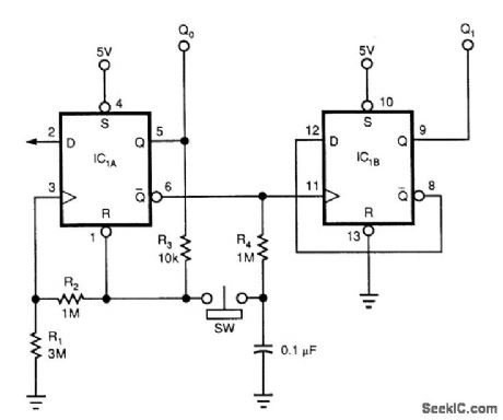
Although this circuit uses a 74HC74, any CMOS variant of this flip-flop will work. IC1A acts as a true/ complement buffer. RI and R2 ensure that IC1A comes out of reset before the clock's edge occurs. R3 applies IC1A's logic state to pins 1 and 3. When the switch closes, the next logic state stored on the capaci-tor transfers to the flip-flop's reset and clock inputs. Releasing the switch lets the capacitor charge to the next state via R4. IC1A's output is the LSB; IC1B's output is the MSB.
Notice that the counter's state advances when the switch is first pressed, rather than when it's released; the latter is the case with many other switch-debouncing schemes. lbu can replace RI with a 22-pF capacitor to reduce the circuit's sensitivity to parasitic effects. The addition of this capacitor also lets you !ower the magnitude of R2 and R3 by a factor of 10. (View)
View full Circuit Diagram | Comments | Reading(3180)
CHILD_PROOF_RESET_SWITCH
Published:2009/7/9 23:14:00 Author:May
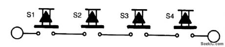
The reset switch on a computer is very important. If an operating instruction threatens to wreck the internal management of a computer, the reset button is often the only way of avoiding a possible disaster. On the other hand, it also could cause a disaster.
It is particularly important that children or pets cannot inadvertently operate the control. The circuit proposed here should put an end to your worries in this respect. Instead of one reset switch, it is necessary to press four switches simultaneously. The chances of this happening via accident, child, or pet are negligible.
The four switches are placed in positions that make it impossible to operate them all with one hand.Instead, two of them can be operated with the fingers of one hand and the other two with the fingers on the other hand. As shown, the four switches are connected in series and are intended to replace the exist-ing switch. (View)
View full Circuit Diagram | Comments | Reading(712)
SIMPLE_BURGLAR_ALARM_WITH_NC_SWITCHES
Published:2009/7/9 21:46:00 Author:May
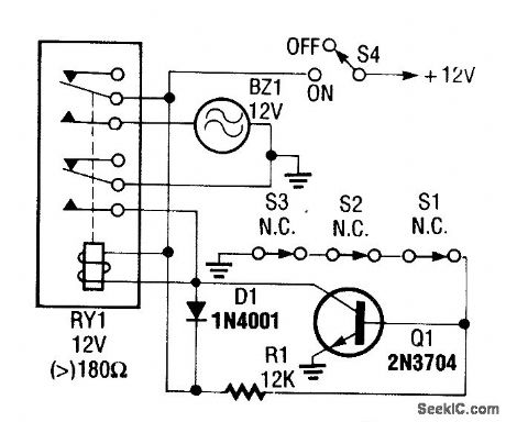
This relay draws 1 mA of idling current. Q1 detects open switch and energizes RY1. (View)
View full Circuit Diagram | Comments | Reading(708)
PROXIMITY_SWITCH
Published:2009/7/9 21:29:00 Author:May
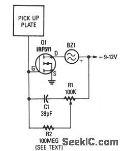
A 3- x -3-inch piece of circuit board, or similar size metal object which functions as the pick-up sensor, is connected to the gate of Q1. A 100-MΩ resistor, R2, isolates Q1's gate from R1, allowing the input impedance to remain very high. If a 100-MΩ resistor cannot be located, just tie five 22-MΩ resistors in series and use that combination for R2. In fact, R2 can be made even higher in value for added sensitivity.Potentiometer R1 is adjusted to where the piezo buzzer just begins to sound off and then carefully backs off to where the sound ceases. Experimenting with the setting of R1 will help in obtaining the best sensitivity adjustment for the circuit.Resistor R1 can be set to where the pick-up must be contacted to set off the alarm sounder. A relay or other current-hungry component can take the place of the piezo sounder to control most any extemal circuit. (View)
View full Circuit Diagram | Comments | Reading(0)
BATTERY_SAVING_DISCONNECT_SWITCH
Published:2009/7/9 20:52:00 Author:May
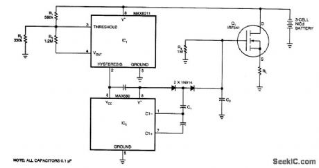


At a predetermined level of declining terminal voltage, the circuit disconnects the battery from the load and halts potentially destructive battery discharge. Q1, a high-side, floating-source MOSFET, acts as the switch. The overall circuit draws about 500 μA when the switch is closed and about 8 μA when it's open.
The values of Ry, R2, and R3 set the upper and lower voltage thresholds, Vu and Vy,, according to the relationships
For the circuit to start,V+ must exceed Vu. The voltage detector IC1 then powers IC2, but only while V+ remains above VL. Otherwise, IC2 loses its power, removes gate drive from Q1, and turns it off. IC2 is a dual charge-pump inverter that normally converts 5 V to ±10 V. Capacitors C1, C2, and the two associated diodes form a voltage tripler that generates a gate drive for Q1 that is approximately equal to two times the battery voltage.
With the values in the schematic, the circuit disconnects 3-cell Nicad battery from its load when V+ reaches a VL of 3,1 V. Approximately 0.5 V of hysteresis prevents the switch from turning on immediately when the circuit removes the load; V+ must first return to Vu, which is 3.6 V. The gate drive declines as the battery voltage declines, cause the ON-resistance of Q1 to reach a maximum of approximately 0.1 Ω, just before Y+ reaches its 3.1-V threshold. A 300-mA load current at that time will cause a 30-mV drop across the disconnect switch, The drop will be 2 to 3 mV less for higher battery voltages. Resistor R4 ensures that Q1 can adequately turn off by providing a discharge path for C2. (View)
View full Circuit Diagram | Comments | Reading(1283)
IR_REFLECTION_PROXIMITY_SWITCH
Published:2009/7/9 20:50:00 Author:May
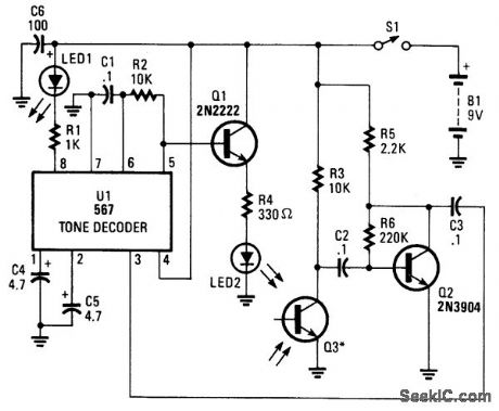
IR radiation from LED2 (modulated by a 1-kHz wave) is keyed by U1, and Q1 is radiated. Reflected IR energy is picked up by Q3, and the audio signal from Q3 is amplified by Q2 and sent to the decoder. The LED1 lights to indicate presence of reflected IR. LED1 can be the input of an isolator so that a triac or SCR can be controlled. (View)
View full Circuit Diagram | Comments | Reading(1076)
HIGH_PERFORMANCE_VIDEO_SWITCH
Published:2009/7/9 3:09:00 Author:May

This figure shows a one-of-two switch with a summing amplifier. The video source's line can be termi-nated either externally or internally to switch R0. With this termination resistor, a load change of less than 1 Ω will be seen by the source when the switch changes state. For this reason, input isolation amplifiers are not necessary. R4 can be varied to control circuit gain, but should never be less than 1400 Ω since the NE5539 is internally compensated for gain values greater than seven. A value of approximately 2500 Ω for R4 will set circuit gain to near unity. Additionally, the circuit output impedance is set by R6, and R5 sets the output dc offset to near zero. (View)
View full Circuit Diagram | Comments | Reading(864)
AUTOMATIC_VIDEO_SWlTCH
Published:2009/7/9 3:06:00 Author:May

Turn on a game, computer, videodisc player, or whatever, and its output takes priority over the antenna-derived signal-the antenna is disconnected and the alternate source is fed to the monitor. When the alternate video source is no longer detected, the switch automatically reconnects the antenna. When the rf carrier is detected, a high logic output appears at pin 15 of U1-squelch status. The signal is then buffered to VMOS FET Q1. This FET can drive CMOS inverter/buffer U2, can be an open-drain output to drive a relay, or can convert to a 5 V logic level. When pin 15 of U1 becomes high, Q1 turns on, pulling pin 11 of U2e low; in turn, pin 12 becomes high. The output of U2e is fed to U2f, forcing its output, at pin 15, low. When the signal at U2 pin 12 is high, D1 is biased on, allowing the signal at J3 to flow through C14, D1, and out to J2 through C13. When the signal at J3 is removed, U1 pin 15 decreases. That decrease causes U2 pin 12 to decrease and U2 pin 15 to increase. When the signal at U2 pin 15 is high, it biases D2 on, allowing the signals at J1 to flow through C12, D2, and out to J2 through C13. (View)
View full Circuit Diagram | Comments | Reading(1261)
GENERAL_PURPOSE_VIDEO_SWITCH
Published:2009/7/9 2:54:00 Author:May
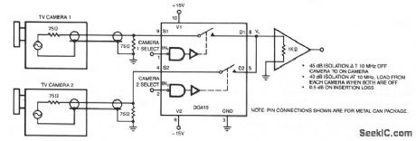
The circuit shown provides 40-dB isolation at 6 MHz and is good for general purpose video switching. (View)
View full Circuit Diagram | Comments | Reading(0)
VIDEO_SWITCH_WITH_VERY_HIGH_OFF_ISOLATION
Published:2009/7/9 2:22:00 Author:May
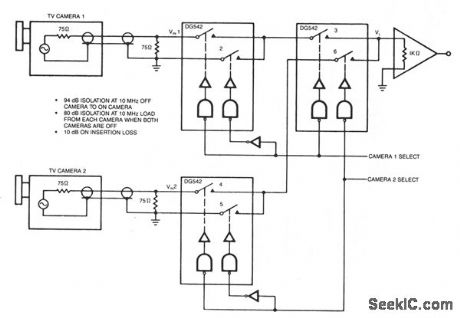
View full Circuit Diagram | Comments | Reading(696)
SOLID_STATE_ZERO_VOLTAGE_SWITCHING_ZVS_CIRCUITS
Published:2009/7/8 22:26:00 Author:May

This circuit is effective for lamp and heater loads. Some circuits driving reactive loads require integral cycling and zero-voltage switching-when an identical number of positive and negative half cycles of voltage are applied to the load during a power period. The circuit, although not strictly a relay because of the three-terminal power connection, performs the integral cycle ZVS function when interfaced with the previous coil circuits.
Fiber optics offers advantages in power control systems. Electrical signals do not flow along the non-conducting fiber, minimizing shock hazard to both operator and equipment. EMI/RFI pick up on the fiber is nonexistent-although high gain receiver circuits might require shielding, eliminating noise pick-up errors caused by sources along the cable route. Both ac and dc power systems can be controlled by fiber optics using techniques similar to the optoisolator solid-state relay. Triac triggering is accomplished through the C106BX301, a low gate trigger current SCR, switching line voltage derived current to the triac gate via the full-wave rectifter bridge. The primary difference between ftber optics solid-state relay circuits and optoisolator circuits is the gain; photo currents are much smaller.
(View)
View full Circuit Diagram | Comments | Reading(1288)
HIGH_VOLTAGE_AC_SWITCHER
Published:2009/7/8 22:19:00 Author:May
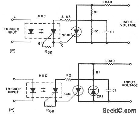
A guide for selecting the component values would consist of the following steps:
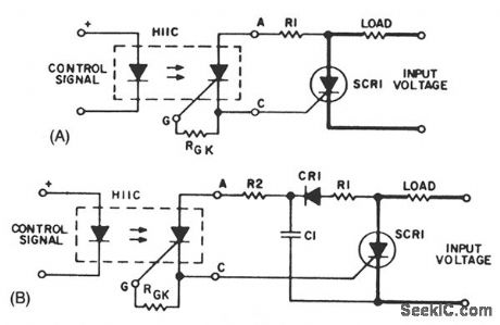
· Choose C1 in a range of 0.05 to 1 μR The maximum value might be limited by the recharging time constant (RL + R1) C1 while the minimum value will be set by the minimum pulse width required to ensure SCR latching.· R2 is determined from peak gate current limits, if applicable, and minimum pulse width requirements.· Select a zener diode. A 25-V zener is a practical value, since this will meet the usual gate requirement of 20 V and 20 Ω. This diode will also eliminate spurious triggering because of voltage transients.· Photon coupler triggering is ideal for the SCR's driving inductive loads. By ensuring that the LASCR latches on, it can supply gate current to SCR1 until it stays on.· Component values for dc voltage are easily computed from the following formulae: EIN-VZR1 = — IG where: V =zener voltage P(R1) =IG·(EIN-VZ) P(ZENER) =IG·VZ (View)
View full Circuit Diagram | Comments | Reading(0)
_HIGH_VOLTAGE_AC_SWITCHER
Published:2009/7/8 22:16:00 Author:May
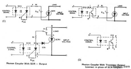
In Fig. 67-1C, R1 can be connected to Point A, which will remove the voltage from the coupler after SCR1 is triggered, or to Point B so that the coupler output will always be biased by input voltage. The former is preferred since it decreases the power dissipation in R1. A more practical form of SCR triggering is shown in Fig. 67-1F. Trigger energy is obtained from the anode supply and stored in C1. Coupler voltage is limited by the zener voltage. This approach permits switching of higher voltages than the blocking voltage capability of the output device of the photon coupler. To reduce the power losses in R1 and to obtain shorter time constants for charging C1, the zener diode is used instead of a resistor. (View)
View full Circuit Diagram | Comments | Reading(737)
HIGH_VOLTAGE_AC_SWITCHER
Published:2009/7/8 22:13:00 Author:May
A basic circuit to trigger an SCR is shown in Fig. 67-1A. This circuit has the disadvantage that the blocking voltage of the photoncoupler output device determines the circuit-blocking voltage, irrespective of higher main SCR capability.
Adding capacitor C1 to the circuit, as shown in Fig. 67-1B, will reduce the dV/dt seen by the photon-coupler output device. The energy stored in C1, when discharged into the gate of SCR1, will improve the di/dt capability of the main SCR.
Using a separate power supply for the coupler adds flexibility to the trigger circuit; it removes the limitation of the blocking voltage capability of the photon-coupler output device. The flexibility adds cost and more than one power supply nftght be necessary for multiple SCRs if no common reference points are available. (View)
View full Circuit Diagram | Comments | Reading(963)
Triac_control_circuit_using_an_ECG776_zero_voltage_switch_IC
Published:2009/7/21 4:48:00 Author:Jessie
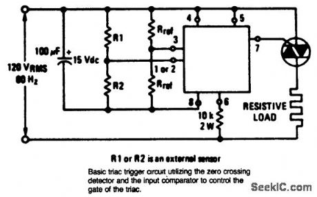
Triac control circuit using an ECG776 zero voltage switch IC. Resistor R2 must be the external sensor for the internal short and open protection to be operative. Select the triac from the ECG5600 series for the particular application (courtesy GTE Sylvania Incorporated). (View)
View full Circuit Diagram | Comments | Reading(2320)
SIMPLE_LOW_COST_RF_SWITCH
Published:2009/7/8 4:13:00 Author:May
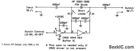
When the digital logic level at the control input is low, the PIN diode is forward-biased by the CMOS gates. The two 1-KΩ bias resistors limit this current to the PIN diode's safe forward current limit. In this state, the switch is on. When the control input is high, the diode is reverse-biased and the switch is off.This switch is well-suited for electronically steered antenna arrays, multiple path switching, and other applications requiring small, low-cost rf switches. This particular design was used in a four-pole rotary switch for a Doppler-shift radio direction-finder operating at 144 MHz.
(View)
View full Circuit Diagram | Comments | Reading(949)
TOUCH_SWITCH
Published:2009/7/8 3:54:00 Author:May
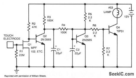
This touch-actuated switch stays on as long as you keep your finger on the touch plate. R1 sets the input impedance to a high 22 M Ω. Q1 picks up stray signals coupled through your body to the touch plate and amplifies them to tum on Q2, which tums on lamp drivers Q3 and Q4. Lamp I1 is any small 12-V lamp, such as a No. 53-12 V 120 mA. R4 and C1 add a small amount of hysteresis (delay) to keep the light from constantly flickering. A relay can be used for I1. (View)
View full Circuit Diagram | Comments | Reading(0)
LINE_HUM_TOUCH_SWITCH
Published:2009/7/8 3:47:00 Author:May
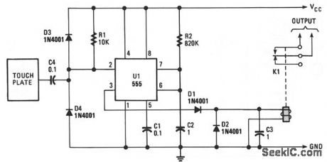
The monostable period is set for about 1 second, as is the usual case. The induced line hum comes through C2, providing a continuous string of trigger pulses. The output becomes low for about 10 ms per second as the monostable times out and then retriggers. Diode Dl and capacitor C3 buffer the relay so it doesn't chatter on those 10-ms pulses. Resistor R2 sets the sensitivity.The relay energizes when the plate is touched and de-energizes, up to one second after the finger is removed. The delay is a function of when the monostable last retriggered. (View)
View full Circuit Diagram | Comments | Reading(1037)
| Pages:7/15 123456789101112131415 |
Circuit Categories
power supply circuit
Amplifier Circuit
Basic Circuit
LED and Light Circuit
Sensor Circuit
Signal Processing
Electrical Equipment Circuit
Control Circuit
Remote Control Circuit
A/D-D/A Converter Circuit
Audio Circuit
Measuring and Test Circuit
Communication Circuit
Computer-Related Circuit
555 Circuit
Automotive Circuit
Repairing Circuit