
Switch Control
Index 9
SOLID_STATE_STEPPING_SWITCN
Published:2009/7/6 20:10:00 Author:May
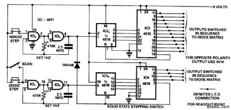
This circuit was designed to make switching of a 48-channel mobile transceiver safe to operate while mobile. The oscillators allow for single-stepping or a scanning function.The scan facility allows for stepping through all 48 channels to check for occupancy or otherwise, and each output is indicated with an LED and labeled accordingly, so at-aglance indication is possible. With full scope of this circuit it is possible to scan 256 channels and by adding more 4 to 16 line encoders etc. you could switch to any required number. (View)
View full Circuit Diagram | Comments | Reading(1680)
ISOLATED_THRESHOLD_SWITCH
Published:2009/7/6 7:43:00 Author:May
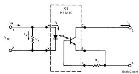
Standard photocoupler programmed with 150-ohm resistor R1 provides threshold switching function for separating high-level noise from switching-signal pulses as short as 10μs. Current-transfer ratio of phototransistor coupler is made practically zero at some arbitrary input current, and changed rapidly back to 10% or more at slightly higher level. Programming range for threshold value extends from 60 mA for 10 ohms at R1 to 3 mA for 400 ohms. Use of 2.7-megohm resistor R2 across base-emitter terminals of coupler reduces low-current gain of phototransistor. Noise currents up to 5 mA on sensing line are rejected while operating currents as low as 10 mA are accepted.-J. Cook, Photocoupler Makes an Isolated Threshold Switch, EDN Magazine, Oct. 5, 1974, p 72, 74, and 76. (View)
View full Circuit Diagram | Comments | Reading(933)
FAST_OPTICALLY_ISOLATED_SWITCH
Published:2009/7/6 7:14:00 Author:May
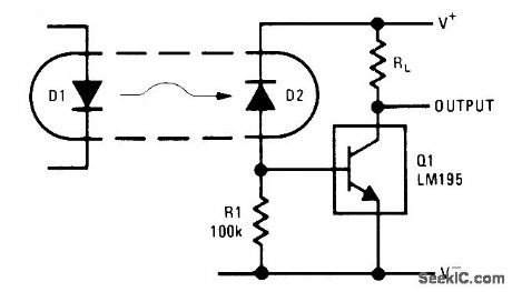
Uses almost any standard optoisolator. Less than 20μA is needed from photodiode D2 to tum LM195 power transistor fully on. Returning cathode of D2 to separate positive supply rather than to collector of al eliminates collector-base capacitance of diode and increases switching speed to 500 ns for 40-V 1-A load.-R. Dobkin, Fast IC Power Transistor with Thermal Protection, National Semiconductor, Santa Clara, CA, 1974, AN-110, p 5. (View)
View full Circuit Diagram | Comments | Reading(916)
SOUND_ACTIVATED_SWITCH
Published:2009/7/6 5:52:00 Author:May

The audio from Mia is amplified by Q1. Peaks of signal (adjusted by R1) greater than about 0.7 volts trigger the SCR and light lamp I1. (View)
View full Circuit Diagram | Comments | Reading(0)
COURTESY_LIGHT_DELAY_SWITCH
Published:2009/7/6 2:15:00 Author:May
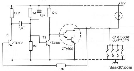

This circuit holds on the internal light for approximately one minute after the car doors are closed. When the door contacts open, a + VE pulse is applied to the base of T1. This transistor turns on, turning off T2 and charging the 10-μF capacitor. T3 turns on, holding on the intemal light . The capacitor takes one minute to discharge when the circuit reverts to its original state. (View)
View full Circuit Diagram | Comments | Reading(808)
5_V_AT_5_A_WITH_IC_SWITCHER
Published:2009/7/6 2:12:00 Author:May
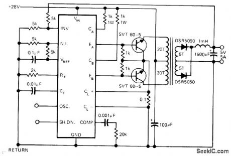
Uses Silicon General SG1524 IC as pulse-width-modulated regulator for which operating frequency remains constant, with ON time of each pulse adjusted to maintain desired output voltage. Operating range extends above 100 kHz but device draws only 10 mA. IC includes voltage reference, oscillator, comparator, error amplifier, current limher, pulse-steering flip-flop, and automatic shutdown for overload.-P. Franson, Today's Monolithic Switching Circuits Greatly Simplify Power-Supply Designs, EDN Maga-zine, March 20, 1977, p 47-48, 51, and 53. (View)
View full Circuit Diagram | Comments | Reading(2135)
FET_DUAL_TRACE_SCOPE_SWITCH
Published:2009/7/5 23:04:00 Author:May
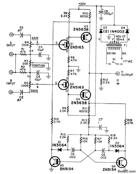
The switcher output goes to the single vertical input of the scope,and a sync line from one of the Inputs is taken to the scope's external-Sync Input.Frequency response of the input amplifiers is 300 kHz over the range of the gain controls.With the gain controls wide open so no attenuatjon of the signal takes place,the frequency response is up to 1 MHz (View)
View full Circuit Diagram | Comments | Reading(1168)
ZERO_CROSSING_SWITCH
Published:2009/7/5 22:34:00 Author:May
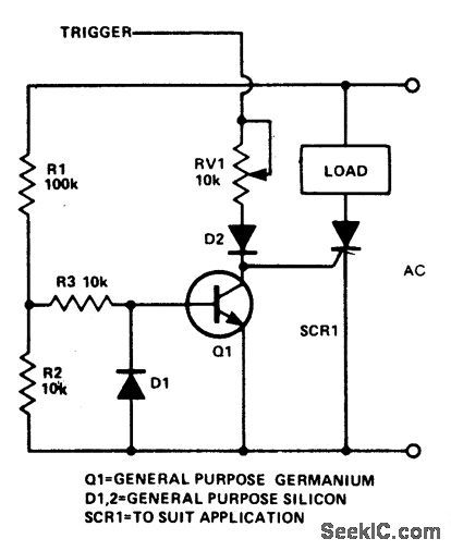
When switching loads with the aid of a thyristor, a large amount of RFI can be generated unless some form of zero crossing switch is used. The circuit shows a simple single transistor zero crossing switch. R1 and R2 act as a potential divider. The potential at their junction is about 10% of the ac voltage. This voltage level is fed, via R3, to the transistor's base. If the voltage at this point is above 0.2, the transistor will conduct, shunting any thyris-tor gate current to ground. When the line po-tential is less than about 2 V, it is possible to trigger the thyristor. The diode D1 is to re-move any negative potential that might cause reverse breakdown. (View)
View full Circuit Diagram | Comments | Reading(4097)
TIME_DELAY_SWITCH
Published:2009/7/2 4:30:00 Author:May
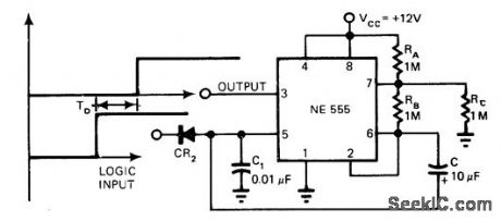
Oscillator connection shown for 555 timer provides delay for switching action controlled by logic input. When logic input is 0 V, timer output is low. When logic input goes high, output remains low for delayof 0.693RBC s and then switches high. Output remains high as long as input is high.-K. D.Dighe, Rearranged Components Cut 555's lnitial-Pulse Errors, EDNMagazine, Jan. 5, 1978, p 82 and 84. (View)
View full Circuit Diagram | Comments | Reading(1022)
SOUND_ACTIVATED_SWITCH
Published:2009/7/2 3:20:00 Author:May
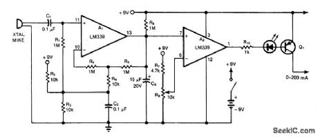
Can be used as sensor for burglar alarm or for turning on su'-veillance tape recorder to monitor conversa-tions. R8, is adjusted to give desired sensitivity at which A2, triggers switch Q1, to provide 200-mA load current and turn on indicator LED. First section of LM339 quad comparator serves as amplifier and detector providing gain of 100. Second comparator compares DC output of first with reference level selected by R8.-D. ft. Mor-gan, Sound Turns Switch On, EDN Magazine, Aug. 5, 1978, p 82 and 84. (View)
View full Circuit Diagram | Comments | Reading(3355)
PUSH_ON_PUSH_OFF_ELECTRONIC_SWITCH
Published:2009/7/1 21:01:00 Author:May
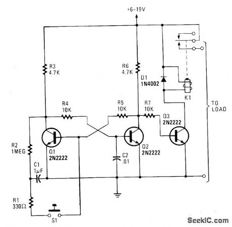
Transistors Q1 and Q2 make up the flip-flop while Q3 drives a reed relay. When powe is first applied to the circuit, Q1 and Q3 are conducting and Q2 is cut off.Momentarily closing S1 causes the flip-flop to switch states-Q1 cuts off and Q2 conducts.When Q2 is conducting, its collector drops to around 0.6 volt. That prevents base current from flowing into Q3 so it is cut off, de-energizing relay K1. The flip-flop changes state every time S1 is pressed. Capacitors C1 and C2 ensure that Q1 is always the transistor that turns on when power is first applied to the circuit. When power is first applied to the basic flip-flop, the initial status is random-Q1 and Q2 both try to conduct and, usually, the transistor with the higher gain will take control, reaching full conduction and cutting off the other one. However, differences in the values of the collector and coupling resistors will also influence the initial state at power-on. With C2 in the circuit, it and R4 form an R-C network that slightly delays the rise in Q2's base voltage. That glves Q1 sufficient time to reach saturation and thus take control. (View)
View full Circuit Diagram | Comments | Reading(6554)
SPEED_SWITCH
Published:2009/7/1 21:01:00 Author:May
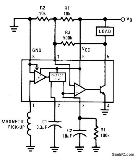
National LM2907 tachometer IC is used as switch to energize load when input frequency exceeds value corresponding to predetermined speed limit. Automotive applications include use as overspeed warning that activates audible and/or visual indicator when auto speed exceeds legal limit or other desiredvalue. Another application is increasing intensity of auto or taxi horn above predetermined speed such as 45 mph. Input is variable-reluctance magnetic pickup positioned against teeth of gear wheel; in typical setup, pickup output is 16.6 Hz at 60 mph. Values shown for comparator-controlling components R1 and C1 (below IC) give switching operation at about 16.6 Hz at input. Report gives design procedure for other frequencies.- Linear Applications, Vol. 2, National Semiconductor, Santa Clara, CA, 1976, AN-162, p 8. (View)
View full Circuit Diagram | Comments | Reading(0)
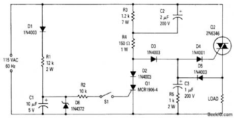
SYNCHRONOUS_PHOTOELECTRIC_SWITCH
Published:2009/7/1 1:43:00 Author:May
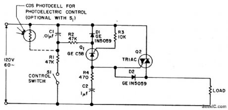
Synchronous switching is turning on only at the instant the ac supply voltage passes through zero, and turning off only when ctyrent passes through zero. This circuit provides this function in response to either a mechanical switch or a variable resistance such as a cadmium-sulfide photocell. This circuit produces the minimum disturbance to the power supply when switching, and always conducts an integral number of whole cycles. It is ideal for use wherever RFI and audio filtering is undesirable, where magnetizing inrush current of transformers causes nuisance fuse-blowing, and where sensitive equipment must operate in the vicinity of power switches. (View)
View full Circuit Diagram | Comments | Reading(1156)
TRIAC_ZERO_POINT_SWITCH
Published:2009/7/1 1:21:00 Author:May
On the initial part of the positive half cycle, the voltage is changing rapidly from zero causing a large current to flow into capacitor C2. The current through C2 flows through R4, D3, and D4 into the gate of the TRIAC Q2 causing it to turn on very close to zero voltage. Once Q2 turns on, capacitor C3 charges to the peak of the line voltage through D5. When the liqe voltage passes through the peak, D5 becomes reverse-biased and C3 begins to discharge through D4 and the gate of Q2. At this time the voltage on C3 lags the line voltage. When the line voltage goes through zero there is still some charge on C3 so that when the line voltage starts negative C3 is still discharging into the gate of Q2. Thus Q2 is also turned on near zero on the negative half cycle. This operation continues for each cycle until switch 51 is closed, at which time SCR Q1 is turned on.Q1 shunts the gate current away from Q2 during each positive half cycle keeping Q2 from turning on. Q2 cannot turn on during the negative cycle because C3 cannot charge unless Q2 is on during the positive half cycle. (View)
View full Circuit Diagram | Comments | Reading(1196)
PHOTOELECTRIC_SWITCH
Published:2009/6/30 23:51:00 Author:May
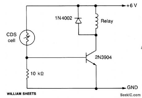
The CDS cell resistance decreases in the presence of light, turning on the 2N3904 relay driver. (View)
View full Circuit Diagram | Comments | Reading(3542)
LIGHT_OPERATED_SWITCH
Published:2009/6/30 23:50:00 Author:May
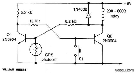
This circuit uses a flip-flop arrangement of Q1 and Q2. Normally Q1 is conducting heavily. Light on CDS photocell causes Q1 bias to decrease, cutting it off, tuming on Q2, removing the remaining bias from Q1. Reset is accomplished by depressing S1. (View)
View full Circuit Diagram | Comments | Reading(799)
ULTRASONIC_SWITCH
Published:2009/6/30 3:12:00 Author:May
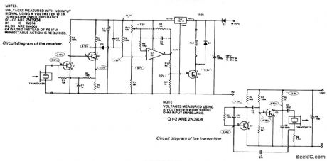
Receiver. Output from the transducer is amplified by Q1 and Q2, and rectified by D1. Voltage on pin 2 of IC1 will go more negative as the input signal increases. IC1 is used as a comparator and checks the voltage on pin 2 (i.e., the sound level), to that on pin 3 which is the reference level. If pin 2 is at a lower voltage than pin 3 (i.e., a signal is present), the output of IC1 will be high (about 10.5 volts) and this will turn on Q3 which will close the relay. The converse occurs if pin 2 is at a higher voltage than pine 3.Transmitter. The oscillator frequency is determined by the transducer characteristics [(minimum (series resonance) at 39.8 kHz fol-lowed by a maximum (parallel resonance) at 41.5 kHz.)] Two transistors from a noninvert-ing amplifier and positive feedback is supplied via the transducer, R6 and C3. At the series resOnant frequency, this feedback is strong enough to cause oscillation. (View)
View full Circuit Diagram | Comments | Reading(945)
9_BIT_USING_DIGITAL_SWlTCHES
Published:2009/6/30 2:58:00 Author:May
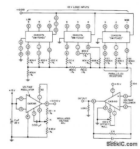
Combination of CD4007A multiple-switch CMOS ICs, ladder network of discrete metal-oxide film resistors, CA3160 voltage-follower opamp, and CA3085 voltage regulator gives digital-to-analog converter that is readily interfaced with 10-V logic levels of CMOS input. Required resistor accuracy, ranging from ±0.1% for bit 2 to ±1% for bits 6-9, is achieved by using series and parallel combinations of 806K resistors.— Linear Integrated Circuits and MOS/FET's, RCA Solid State Division, Somerville, NJ, 1977, p 267-268. (View)
View full Circuit Diagram | Comments | Reading(975)
MALE_FEMALE_VOICE_SWITCH
Published:2009/6/30 1:39:00 Author:May
Circuit developed by NASA engineers to improve intelligibility of voice communication during Apollo moon shots passes only the three portions of the speech spectrum required for clear speech:300-400 Hz and 2500-3000 Hz for both sexes and 900-1700Hz for males or t 100-1900 Hz for females. Pot ad lusts null to about 600 Hz. Circuit improves readabilhy of weak DX voice signals in noise.-J. Fisk, Circuits and Techniques, Ham Radio, June 1976, p 48-52. (View)
View full Circuit Diagram | Comments | Reading(839)
REMOTE_ON_OFF_SWITCH
Published:2009/6/29 3:47:00 Author:May
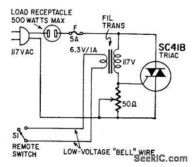
This circuit provides power control with-out running line-voltage switch leads. The primary of a 6-volt filament transformer is con-nected between the gate and one of the main terminals of a triac. The secondary is connected to the remote switch through ordinary low-voltage line. With switch open, transformer blocks gate current, prevents the triac from firing and applying power to the equipment. Closingthe switchshort-circuits the secondary, causing the transformer to saturate and trigger the triac. (View)
View full Circuit Diagram | Comments | Reading(1185)
| Pages:9/15 123456789101112131415 |
Circuit Categories
power supply circuit
Amplifier Circuit
Basic Circuit
LED and Light Circuit
Sensor Circuit
Signal Processing
Electrical Equipment Circuit
Control Circuit
Remote Control Circuit
A/D-D/A Converter Circuit
Audio Circuit
Measuring and Test Circuit
Communication Circuit
Computer-Related Circuit
555 Circuit
Automotive Circuit
Repairing Circuit