
Switch Control
Index 4
DIFFERENTIAL_ANALOG_SWITCH
Published:2009/7/14 0:45:00 Author:May
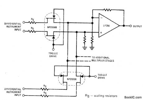
NPD5566 dual JFETs provide high accuracy for differential multiplexer because JFET sections track at better than ±1% over wide temperature range, close tracking reduces errors due to common-mode signals Values of resistors depend on application and on type of opamp used.- FET Databook, National Semiconductor, Santa Clara, CA, 1977, p 6-26-6-36. (View)
View full Circuit Diagram | Comments | Reading(0)
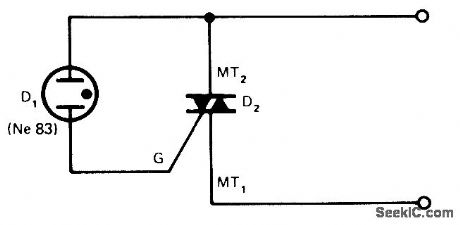
SΥNCHRONOUS_SWITCH
Published:2009/7/14 0:30:00 Author:May
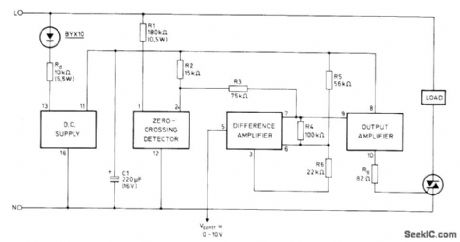
Mullard TCA280A trigger module provides triggering of load triac at zero crossings of AC line voltage. Values shown are for triac requiring gate current of 100mA; for other triacs, values of Rd, Rg, and C1 may need to be changed. Designed for resistive loads and ON/OFF rather than propoltional control.- TCA280A Trigger IC for Thyristors and Triacs, Mullard, London, 1975, Technical Note 19, TP1490, p 10. (View)
View full Circuit Diagram | Comments | Reading(1252)
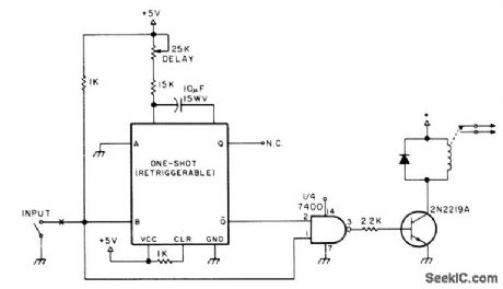
SOUND_OPERATED_SWITCH
Published:2009/7/13 23:46:00 Author:May
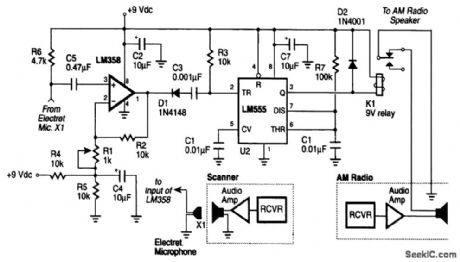
An electret microphone is placed directly in front of the scanner speaker. When the microphone (X1) picks up sound (usually voice) from the speaker, the sound signal is amplified and detected, activates a retriggerable one-shot circuit, and controls the relay (K1). The relay controls the AM radio speaker, muting it when sound is detected from the scanner. (View)
View full Circuit Diagram | Comments | Reading(0)
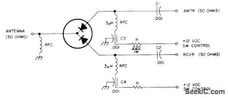
RF_SENSING_TB_SWITCH
Published:2009/7/13 23:43:00 Author:May
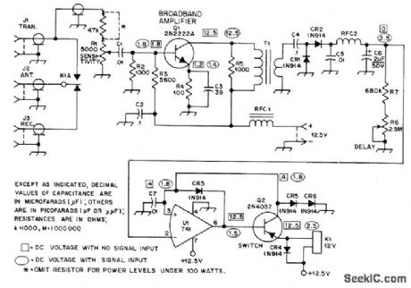
System detects presence of RF at output of transmitter and changes antenna connection from receiver to transmitter instantly and automatically. No modifications are required for transmitter or receiver. RF voltage divider R1 permits use with transmitters of any power. Broadband amplifier Q1 feeds voltage doubler CRl-CR2 through broadband toroidal step-down transformer T1.CR6, R7, and R6 form adjustable timing network that governs hold-in time of relay K1. Inverting amplifier U1 turns on Q2 for energizing K1 and switching antenna to transmitter when RF is sensed. When no rectified RF reaches UI, Q2 is cut off and antenna is changed over to receiver. RFC1 and BFC2 have 42 turns No. 28 enamel on Amidon FT-50-43 core, T1 uses Amidon FT-50-43 core, with 25turns No. 28 enamel for primary and 5 turns No. 28 over this for secondary.-D. DeMaw and J. Rusgrove, An RF-Sensed Antenna Changeover Relay, 0ST, Aug. 1976, p 21-23. (View)
View full Circuit Diagram | Comments | Reading(1582)
SOUND_ACTIVATED_SWITCH
Published:2009/7/13 23:39:00 Author:May
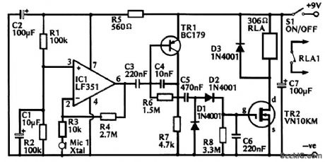
The circuit uses IC1 as a low-noise preamplifier with a voltage gain of 270 times. This is followed by a second stage of amplification, which produces a similar voltage gain. The second stage uses TR1 in the common-emitter mode; this is a conventional arrangement, except for the inclusion of C4. This capacitor provides a considerable amount of high-frequency attenuation, which is necessary in order to prevent instability. Capacitor C5 couples the greatly amplified output of TR1 to a rectifier and smoothing circuit, which gives a positive dc output signal that is roughly proportional to the input-signal level. If the input signal is sufficiently strong, the bias voltage at the gate of VMOS device TR2 will be adequate to bias this transistor into conduction, and the relay that forms its drain load is then activated, A pair of normally open relay contacts are used to control whatever item of equipment is operated by the unit. Of course, the voltage at the gate of TR2 soon decays, as C6 discharges through R8 if the input signal ceases, and the relay is then switched off. The decay time is roughly 1 second, which is about the optimum time for most applications. The attack time of the circuit is only a fraction of a second, and the unit responds almost immediately when a sound is initially picked up by the microphone. (View)
View full Circuit Diagram | Comments | Reading(0)
PIN_DIODE_TR_SWITCH
Published:2009/7/13 23:22:00 Author:May
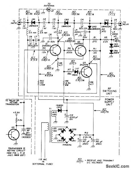
Solid-state TR switch operates at very high keying speeds and handles up to 100 W while transferring antenna between receiver and transmitter in accordance with transmitter keying demands. Uses Unitrode UM4004 PIN diodes to provide about 0.2-dB insertion loss when forward-biased and about 30-dB isolation when reverse-biased. CR1 is forward-biased for about 45 mA DC and CR2 is reverse-biased by 124 V during transmit, for minimum loss in CR1 and maximum isolation in CR2. Circuit is designed to operate from collector of keying-circuit transistor in Touchcoder II (in dotted lines at lower left), but any source providing required T (transmit) and R (receive) DC voltages shown on diagram will key circuit. Article covers construction in detail.-J. K. Boomer, PIN Diode Transmit/Receive Switch for 80-10 Meters, Ham Radio, May 1976, p 10-15.
(View)
View full Circuit Diagram | Comments | Reading(2214)
TR_SWITCH
Published:2009/7/13 23:13:00 Author:May
Simple transmit-receive switch uses 74122 retriggerable mono MVBR with clear and one NAND gate. When input of gate goes low (during key down or speech), transistor conducts and closes relay. Relay stays closed for period determined by delay pot, to maintain transmit condition between dots or dashes or between other pauses. Switch may be removed and any other TT'L-compatible input applied at point X.-B. Voight, The TI'L One Shot, 73Magazine, Feb, 1977, p 56-58. (View)
View full Circuit Diagram | Comments | Reading(0)
ZERO_POINT_SWITCH
Published:2009/7/13 22:44:00 Author:May
Used to control resistive loads. With S1 open, triac Q2 is turned on very close to zero on initial part of positive half-cycle because of large current flow into C2.Once Q2 is on, C3 charges through D5. When line voltage goes through zero and starts negative, C3 is still discharging into gate of C2 to turn it on near zero of negative half-cycle. Load current thus flows for most of both half-cycles. When S1 is closed, Q1 is turned on and shunts gate current away from Q2 during positive half-cycles. Q2 cannot turn on during negative half-cycle because C3 cannot charge, which makes load current zero.- Circuit Applications for the Triac, Motorola, Phoenix, AZ, 1971, AN-466, p 12. (View)
View full Circuit Diagram | Comments | Reading(0)
TR_SWITCH
Published:2009/7/13 22:28:00 Author:May
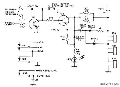
Consists of driver transistors Q1 and Q2 and reed relays K1-K3. K1 switches antenna from receiver to transmitter, K2 grounds receiver input, and K3 keys transmitter. Coil of K1 has 400 turns No. 32 enamel, while K2 and K3 each have 120 tums. Coils are wound directly on glass of reed relays and covered with epoxy cement. LED normally glows dimly, with brightness increasing when character is keyed.-J. H. Fox, An Integrated Keyer/TR Switch, QST, Jan. 1975, p 15-20. (View)
View full Circuit Diagram | Comments | Reading(1474)
125_ns_POWER_SWITCH
Published:2009/7/13 22:13:00 Author:May
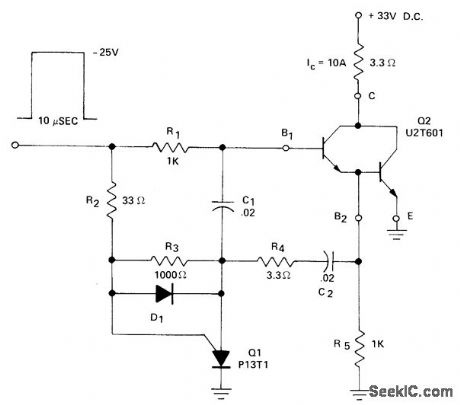
Developed for repetitive pulse applications in which rise, fall, and storage times of pulse must be kept at absolute minimum. Circuit provides very high gain of Unitrode U2T601 Darlington and switching speeds up to 5 times greater than conventional techniques. Load power up to 10 A is typically applied within 125 ns. Applications include drive for laser diode and for radar circuits.- Designer's Guide to Power Darlingtons as Switching Devices, Unitrode, Watertown, MA, 1975, U-70, p 19. (View)
View full Circuit Diagram | Comments | Reading(751)
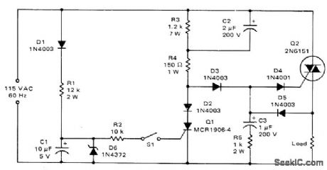
LINE_POWERED_SWITCH
Published:2009/7/13 21:43:00 Author:May
When AC line twitch is closed, power is not applied to load until after line voltage next goes through zero. Identical circuits control each half of AC cycle. Transistor turn-on at 1.4 V prevents SCR from triggering until 0.013 ms (less than one-third electrical degree) after next zero-crossing point.-A. S. Roberts and O. W. Craig, Efficient and Simple Zero-Crossing Switch, EDN|EEE Magazine, Aug. 15, 1971, p 46-47. (View)
View full Circuit Diagram | Comments | Reading(827)
THYRISTOR_SWITCH
Published:2009/7/13 20:52:00 Author:May
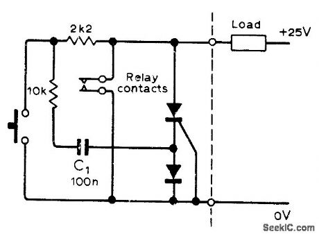
When circuit of conventional P-gate thyristor is grounded by switch, negative-going pulse is applied to thyristor cathode, which reverse-biases the diode. When thyristor conducts, diode is forward-biased and has only about 0.7-V drop. Use low-voltage diode, rated for full load current. Opening of relay contacts makes circuit switch off.-R. V. Hartopp, Grounded Gate Thyristor, Wireless World, Feb. 1977, p 45.
(View)
View full Circuit Diagram | Comments | Reading(1213)
VOLTAGE_SENSITIVE_SWITCH
Published:2009/7/13 20:42:00 Author:May
RCA 40527 triac is triggered by small neon. After breakdown occurs bidirectionally at 88 V, triac takes over as short-circuit. D1 can be any other voltage breakdown device, such as diac or zener, and thyristor can be used in place of triac to give unilateral switching. Applications include use as power crowbar, with breakdown level set by artificial resistance-controlled zener.-L. A. Rosenthal, Breakdown and Power Devices Form Unusual Power Switch, EDN Magazine, July 5, 1974,p74-75. (View)
View full Circuit Diagram | Comments | Reading(1083)
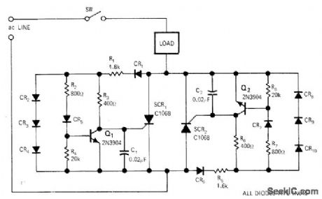
PERFECT_AC_SWITCH
Published:2009/7/13 20:39:00 Author:May
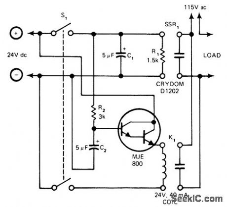
Developed for use in computdrized equipment to prevent generation of severe noise spikes if contact closure can occur at any point in AC cycle. Closing S1 gates solid-state relay SSR1, which noiselessly switches load at next zero crossing. During this time, C2 charges through R2, After time T = 3R2C2, MJE800 Darlington is turned on, pulling in relay K1 to follow up SSR1 with hard contacts.When S1 is later opened, K1 drops out immediately but C1 discharges through gate of SSR1 to hold it on for about T = 6R1C1. Load is then switched off at next zero crossing after this delay.-E. Woodward, This Circuit Switches AC Loads the Clean Way, EDN Magazine, Nov. 20, 1975, p 160 and 162. (View)
View full Circuit Diagram | Comments | Reading(860)
DIODE_TR_SWITCH
Published:2009/7/13 5:19:00 Author:May
Microwave Associates MA8334 solid-state TR switch replaces conventional relays tor switching antenna back and forth between transmitter and receiver. Handles up to 50 W CW at 144 MHz, and can be used at other frequencies up to 1000 MHz by proper choice of circuit constants Measured insertion loss is 0.25 dB,and SWR is 1.23:1 when operated at 50 ohms.-T Reddeck,Solid-State VHFUHF Transmit/Receive Switch,Ham Radio,Feb1978,p 54. (View)
View full Circuit Diagram | Comments | Reading(1931)
TOUCH_SWITCH_3
Published:2009/7/13 4:51:00 Author:May
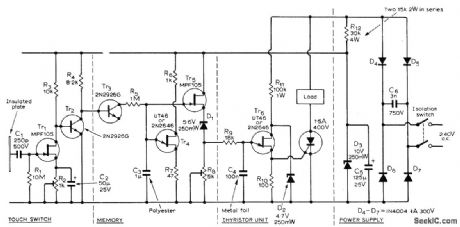
Finger on insulated metal plate applies small AC voltage (picked up by body) to FET Tr1 for amplification, to produce line-frequency square wave across R4 for application to memory section Tr3-Tr5. Charging of C3 through Tr3 and R5 produces DC output voltage across R8 that is fed to UJT Tr6 for triggering thyristor. C4 is discharged at about 10-ms intervals by Tr6 which operates from rectified AC line. For high voltage across R8, such as 4 V, thyristor is triggered early in AC cycle and maximum power is supplied to load. Diodes D4-D7 ensure that control is provided over both positive and negative half-cycles of line. The longer a finger is held on touch switch, the greater is the voltage across R8 and the more current there is through load. Removing finger turns off load, which can be lamps or other electric equipment.-R. Kreuzer, Touch-Switch Controller, Wireless World, Aug. 1971, p 389. (View)
View full Circuit Diagram | Comments | Reading(1005)
DEBOUNCING_TOUCH_SWITCH
Published:2009/7/13 4:47:00 Author:May
Foolproof debouncing for touch switch using toggling flip-flop (half of Motorola MC14013) is provided by two gates connected as monostable pulse stretcher. Time constant of pulse stretcher is selected to match needs of application. For status display, LED driven by 2N3903 transistor can be connected to Q terminal of flip-flop.-V. Gregory, CMOS Touch Switches-Convenient, Less $ and Sexy, EDN Magazine, May 5, 1976, p 112. (View)
View full Circuit Diagram | Comments | Reading(1611)
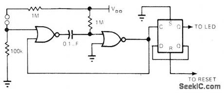
TOUCH_SWITCH_FOR_MUSIC_KEYBOARD
Published:2009/7/13 4:46:00 Author:May
Touching metal sensor plate adds about 300pF of capacitance between plate and ground,changing RC delay network that slows down clock waveform reaehing -D input of 4013 dual D flip-flop, making flip-flop output high for duration of contact. Circuit is repeated for each key in electronic music system.-D. Lancaster, CMOS Cookbook, Howard W. Sams, Indianapolis, IN, 1977, p 278-282. (View)
View full Circuit Diagram | Comments | Reading(1048)
PROXIMITY_SWITCH_1
Published:2009/7/13 4:45:00 Author:May
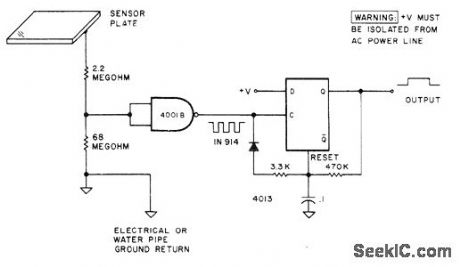
Based on coupling of human body to 60-Hz power line. Hand held close to sensor plate induces hum into 4001B gate. This is squired and used to trip 4013 retriggerable mono MVBR. Output is clean from instant of first proximity until several milliseconds after release. Sensitivity depends on size of plate.-D. Lancaster, Clocked Logic, Kilobaud, May 1977, p 24-30. (View)
View full Circuit Diagram | Comments | Reading(1048)
BICOLOR_LED_SPST_SWITCH
Published:2009/7/13 4:43:00 Author:May
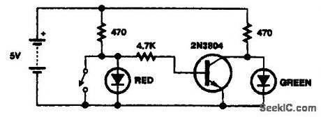
A transistor and a few resistors control two LEDs where the cathodes have a common lead. (View)
View full Circuit Diagram | Comments | Reading(1355)
| Pages:4/15 123456789101112131415 |
Circuit Categories
power supply circuit
Amplifier Circuit
Basic Circuit
LED and Light Circuit
Sensor Circuit
Signal Processing
Electrical Equipment Circuit
Control Circuit
Remote Control Circuit
A/D-D/A Converter Circuit
Audio Circuit
Measuring and Test Circuit
Communication Circuit
Computer-Related Circuit
555 Circuit
Automotive Circuit
Repairing Circuit