
LED and Light Circuit
Index 18
Automatic Night Lamp with Morning Alarm
Published:2012/10/10 1:57:00 Author:muriel | Keyword: Automatic, Night Lamp, Morning Alarm
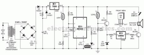
This circuit automatically turns on a night lamp when bedroom light is switched off. The lamp remains ON until the light sensor senses daylight in the morning. A super-bright white LED is used as the night lamp. It gives bright and cool light in the room. When the sensor detects the daylight in the morning, a melodious morning alarm sounds.The automatic night lamp circuit utilises light-dependant resistors (LDRs) for sensing darkness and light in the room. The resistance of LDR is very high in darkness, which reduces to minimum when LDR is fully illuminated. LDR1 detects darkness, while LDR2 detects light in the morning.
Night lamp circuit explanation
When LDR1 is illuminated with ambient light in the room, its resistance remains low, which keeps trigger pin 2 of IC2 at a positive potential. As a result, output pin 3 of IC2 goes low and the white LED remains off. As the illumination of LDR1’s sensitive window reduces, the resistance of the device increases.
In total darkness, the specified LDR has a resistance in excess of 280 kiloohms. When the resistance of LDR1 increases, a short pulse is applied to trigger pin 2 of IC2 via resistor R2 (150 kiloohms). This activates the monostable and its output goes high, causing the white LED to glow.
LDR2 and associated components generate the morning alarm at dawn. LDR2 etects the ambient light in the room at sunrise and its resistance gradually falls and transistor T1 starts conducting. When T1 conducts, melody-generator IC UM66 (IC3) gets supply voltage from the emitter of T1 and it starts producing the melody. The musical tone generated by IC3 is amplified by single-transistor amplifier T2. Resistor R7 limits the current to IC3 and zener diode ZD limits the voltage to a safer level of 3.3 volts.
The night lamp with alarm circuit can be easily assembled on a general-purpose PCB. Enclose it in a good-quality plastic case with provisions for LDR and LED. Use a reflective holder for white LED to get a spotlight effect for reading. Place LDRs away from the white LED, preferably on the backside of the case, to avoid unnecessary illumination. The speaker should be small so as to make the gadget compact.
Night lamp with alarm circuit diagram
(View)
View full Circuit Diagram | Comments | Reading(2088)
Sound controlled lights
Published:2012/10/10 1:56:00 Author:muriel | Keyword: Sound controlled, lights
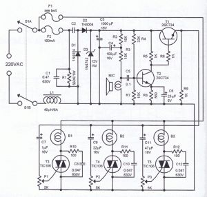
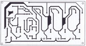
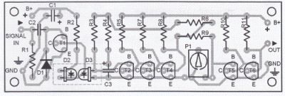
This sound controlled lights circuit design is used to control the brightness of the lights attached to it in sync with the sound that is being capturated by its microphone. This electronic circuit design is very common in disco houses, bars, parties …Usually, sound controlled lights are just connected in parallel with the loudspeakers. This configuration has two disadvantages: first, a very power amplifier can destroy the lights or worse, a defective light can destroy the amp. This problem is avoided by the circuit by not connecting directly to the amp. Instead, it picks up the sound with its microphone.
The power supply part is on the left of the electret microphone amplifier and the light controller part is on the right. The capacitors C2 and C3 are the capacitive voltage divider and reduces the power supply level. Diodes D1 and D2 rectify the positive swing of the AC voltage. The network composed of L1 and C1 protects the power line from voltages surges. In this circuit design, an electret microphone is being used. Take note that there are 2 types of electret mics. The first type has three pins for power, ground, and output. The second type has only two pins. The second type is used for this circuit.
Sound controlled light circuit diagram
In building this sound controlled lights circuit, take note that you are dealing with strong voltages and currents. The components used must have enough ratings to deal with those.The potentiometer P1, P2 and P3 must have plastic shafts and knobs. Use a shielded cable to connect the microphone to the circuit .
All wirings going to the main supply and lights must be isolated with shrink tubings. The case for the circuit must be made of plastic. Do not let anything metallic protrude out of the box.Even the heatsinks for the triacs are electrified. Beware that there is no isolation between this circuit and the main power lines. The maximum power output of each outpuc (triac) is 400 watts, do not exceed that level!
Audio controlled lights PCB Layout
(View)
View full Circuit Diagram | Comments | Reading(2452)
Fuse indicator circuit with light-emitting diode
Published:2012/10/9 21:15:00 Author:Ecco | Keyword: Fuse indicator , light-emitting diode
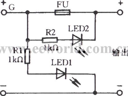
Motors and other electrical equipment commonly use fuse for over current and short circuit protection. But when the fuse blows, and it is not easy to detect. The circuit shown in Figure can timely inform the fuse blown. This is used for DC power fuse indicator. When the power output is normal, the current flows through R1, then LED1 is lit, it only shows that load work normally and supply polarity is normally. At this point, LED2 is fused and in short circuit without emitting light. When the fuse is blown, the current flowing through R2 makes LED2 light to indicate fuse failure.
(View)
View full Circuit Diagram | Comments | Reading(4492)
TSOP 1738 Photo module Design notes
Published:2012/10/9 2:40:00 Author:muriel | Keyword: Photo module

TSOP 17… Series Photomodules are excellent Infrared sensors for remote control applications. These IR sensors are designed for improved shielding against electrical field disturbances.TSOP 1738 Photo module Design notesTSOP 17…. Series Photomodules are miniature IR sensor modules with PIN photodiode and a preamplifier stage enclosed in an epoxy case. Its output is active low and gives +5 V when off. The demodulated output can be directly decoded by a microprocessor. The important features of the module includes internal filter for PCM frequency, TTL and CMOS compatibility, low power consumption (5 volt and 5 mA), immunity against ambient light, noise protection etc. The added features are continuous data transmission up to 2400 bps and suitable burst length of 10 cycles per burst.Inside the Photo moduleThe photo module has a circuitry inside for amplifying the coded pulses from the IR transmitter. The front end of the circuit has a PIN photodiode and the input signal is passed into an Automatic Gain Control(AGC) stage from which the signal passes into a Band pass filter and finally into a demodulator. The demodulated output drives an NPN transistor. The collector of this transistor forms the output at pin3 of the module. Output remains high giving + 5 V in the standby state and sinks current when the PIN photodiode receives the modulated IR signals. Block diagram is given in Fig 1
Pin assignment
Photomodules are 3 pin devices. These pins are assigned for +V,–V and output. The pin assignment of TSOP 17… series from the front side (projected side) is Pin 1 Ground, Pin 2 + 5V and pin 3 Output. The photo module requires regulated 5V supply. If the supply voltage increases, the device will be destroyed.
The pin assignment (Front view) of some common Photomodules
Type pins 1 2 3 Response frequencyTSOP 1730 G 5V OP 30 kHzTSOP 1736 G 5V OP 36 kHzTSOP 1738 G 5V OP 38 kHzTSOP 1756 G 5V OP 56 kHzTSOP 1236 G 5V OP 36.7 kHzTSOP 1838 OP G 5V 38 kHzTSOP 1138 G 5V OP 38 kHzTK 1836 OP G 5V 36 kHzSFH 506-38 G 5V OP 38 kHzRPM 7238F OP G 5V 37.9 kHz
Design considerations
For the proper functioning of the Photo module, it is necessary to consider some important aspects.1. Supply voltage should be + 5 Volts. For this, a 5.1 volt Zener must be connected to the +V pin and ground.2. A 100 uF capacitor should be connected to the +V pin as a buffer and filter capacitor. This will suppress the power supply disturbances.3. Carrier frequency should be close to the center frequency of the band pass filter. 38 kHz in the case of TSOP 1738.4. Burst length must be 10 cycles per burst or more.5. Between each 10 to 70 cycles, a gap time of 14 cycles is necessary to reset the module.6. DC lights such as tungsten bulb and daylight affects the functioning of the photo module.7. Signals from Fluorescent lamps with electronic ballast will affect the working of the photo module.8. Continuous IR signal (non- pulsed) will disturb the photo module and it will not responds to it.
Photo module design is given in Fig.2
(View)
View full Circuit Diagram | Comments | Reading(1807)
LED Optocoupler circuit
Published:2012/10/9 2:36:00 Author:muriel | Keyword: LED Optocoupler
This LED Optocoupler circuit uses two ordinary LEDs as the optocoupler element. When a voltage of 2V is fed to the input, LED 2 will generate a voltage that is strong enough to switch on transistor T5. The upper frequency limit is around 38 kHz. Very low pulse frequencies are almost meaningless for the circuit.Eventhough the LEDs are quite intensive to stray light, it is a good idea to enclose them with an opaque box. Resistor R2 must be selected basing on the power supply voltage. It can be between 680 Ω and 1 KΩ. Resistor R11 must not be lower than 220 Ω.Transistor T6 has an open-collecter character.
Optocoupler Circuit Diagram
Optocoupler PCB and Parts Placement
(View)
View full Circuit Diagram | Comments | Reading(1434)
White LED Flood Lamp circuit
Published:2012/10/9 2:30:00 Author:muriel | Keyword: White LED, Flood Lamp
This White LED lights illuminates your porch with cool white light. The circuit is too simple and energy saving design. Its current consumption is practically nil but can provide light like a 20 watt CFL lamp. It is directly connected to AC lines to eliminate a bulk transformerUltra White LED Lamps are now replacing the fluorescent lamps due to its energy saving property and simplicity of design. White LED emits 1000 to 6000 MCD light and easily works on 3 volts at 20 mA. White LEDs are available as spot light and diffuse type versions. Different sizes like 3mm, 5mm and 10 mm varieties are now common. High watt single white LED is also available. White LEDs was introduced in 1990 which uses Indium Gallium Nitride (InGaN) as the semiconductor. White LED contains a blue chip with white inorganic Phosphor.
When blue light strikes the phosphor, it emits white light. The circuit uses capacitive reactance to drop high volt AC to low volt AC. This reduces power loss due to heat dissipation. The value of the AC capacitor can be calculated using the formula X c= 1/ (2 π f C) where, Xc is the reactance in ohms, C the capacitance in farads and f the mains frequency. Xc = Vrms / I where Vrms is the input voltage and I is the current flowing through LEDs. The low volt AC (around 100 volts) dropped by C1 is then rectified by a full wave rectifier formed of D1-D4.
Capacitor C2 act as a ripple remover and buffer. Zener diode ZD regulates DC to 69 volts and prevents excess reverse voltage across the LEDs during the negative half cycles.R1 is a must in the circuit to bleed the stored current from C1 when the circuit in unplugged. C1 can store more than 400 volts for many days if R1 is not connected. This can give a lethal shock.
R2 reduces the inrush current.20 LEDs are connected as a string to obtain luminance equal to 20W CFL. Enclose the circuit in a shock proof case. If a reflector is provided behind the LEDs, it will give a flood light appearance.
Important! Do not touch any points or trouble shoot when the circuit is connected to mains.
Caution This is an AC powered circuit and can give fatal shock if handled carelessly. Do not construct the circuit unless you are competent to handle high volt circuits.
LED Lights Circuit Diagram
(View)
View full Circuit Diagram | Comments | Reading(1762)
Points, line overflow LED display circuit with LM3914
Published:2012/10/8 21:01:00 Author:Ecco | Keyword: Points, line overflow, LED display
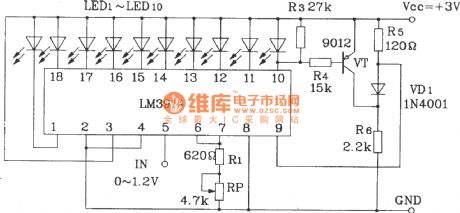
This circuit is in point working mode when it has no overflowing. When it is overflowing, LED changes into line display mode, thus indicating the overflowing.
(View)
View full Circuit Diagram | Comments | Reading(4907)
Basic structure of LED light column display
Published:2012/10/8 21:12:00 Author:Ecco | Keyword: Basic structure , LED, light column , display
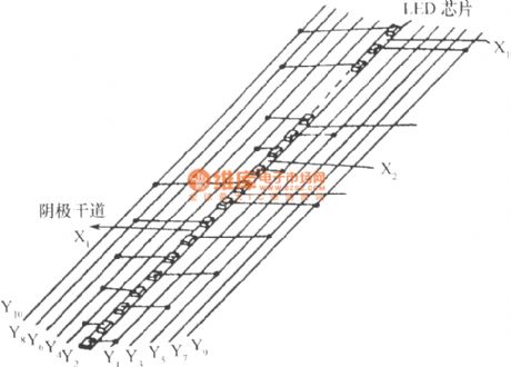
In this structure, high brightness light emitting diode chips are arranged in a straight line, and 100 chips are divided into 10 groups, each group has 10 chips. Each group shares a common cathode, and every anode with the same medium sequence is attached to the anode roads Y1,Y2,...,Y10, 10 cathodes are respectively X1,X2,...,X10, then they constitute a 10x10 matrix. This device works with matrix-scanning mode, so it is called matrix-scanning beam display device. This device also set a chip under zero line of in device settings for indicator.
(View)
View full Circuit Diagram | Comments | Reading(1136)
Christmas lights circuit with optocoupler
Published:2012/10/8 22:25:00 Author:Ecco | Keyword: Christmas lights , optocoupler
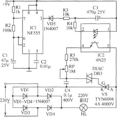
When the power is turned on, the lantern HL is brighter gradually; when it is brightest, it will be darken automatically; if it is darkest, it will be automatically gradually brighter. The whole process is smooth. Lantern HL's luminance change depends on the charging and discharging of the capacitor C3. When the pin 3 of IC1 (NE555) outputs high, capacitor C3 begins to discharge, and the brightness of the lantern HL begins to decline by IC2 (CN25) optical isolation. IC1 here is set astable oscillator, of which frequency is determined by R1, R2 and C1.
(View)
View full Circuit Diagram | Comments | Reading(2230)
Mock Flasher LED circuit
Published:2012/10/8 2:50:00 Author:muriel | Keyword: Mock Flasher, LED
This simple Mock Flasher LED simulates the indicator of a sophisticated Alarm system. It can be placed in doors, gates and vehicles to confuse intruders. The circuit is too simple using a Unijunction transistor as an oscillator.Uni junction transistor (UJT) is an electronic semiconductor device that has only one junction. The UJT has three terminals: an emitter (E) and two bases (B1 and B2). The base is formed by lightly doped n-type bar of silicon. Two ohmic contacts B1 and B2 are attached at its ends. The emitter is of p-type and it is heavily doped. The resistance between B1 and B2, when the emitter is open-circuit is called inter-base resistance. The 2N2646 is the most commonly used version of the UJT.
UJT 2N2646
UJT Pin Connection -Bottom View
Working of UJT
The UJT is biased with a positive voltage between the two bases. This causes a potential drop along the length of the device. When the emitter voltage is driven approximately one diode voltage above the voltage at the point where the P diffusion (emitter) is, current will begin to flow from the emitter into the base region. Because the base region is very lightly doped, the additional current (actually charges in the base region) causes conductivity modulation which reduces the resistance of the portion of the base between the emitter junction and the B2 terminal. This reduction in resistance means that the emitter junction is more forward biased, and so even more current is injected. Overall, the effect is a negative resistance at the emitter terminal. This is what makes the UJT useful, especially in simple oscillator circuits.
Working of Mock Flasher LED
UJT 2N 2646 is used as a simple oscillator with the oscillating components R1 and C2. The LED is connected between the base2 (B2) of the UJT and the ground. Resistor R2 restricts current through the UJT as well as LED. At power on, capacitor C2 charges through R1 and when it fully charges, emitter of UJT forward biases and current flows into the base. LED then lights. The discharge of C2 is followed by its charging again creating an oscillating cycle so that LED flashes.
Mock Flasher LED Circuit Diagram
(View)
View full Circuit Diagram | Comments | Reading(1303)
Flashing Brake Light for Motorcycles circuit
Published:2012/10/8 2:47:00 Author:muriel | Keyword: Flashing, Brake Light
This flashing brake light circuit can be used for motorcycles. When brake-light switch S1 is closed, power is applied to U1 and U2. Two inverters of U2, a 4049 hex inverting buffer, are connected in a low frequency oscillator that feeds clock pulses into U1, a 4017 decade counter/divider. Outputs 0, 2, 4, 6 and 8 of U1 are coupled to the gate of Q1 through a 1N914 diode.As the 4017 counts, it turns the brake light on and off four times and then leaves it on until the brake switch is released. The on/off rate can be set by potentiometer R2.For best results, the on/off rate should be set so that it is rapid.
Flashing Brake Light Circuit Diagram
(View)
View full Circuit Diagram | Comments | Reading(1356)
Flashing Light with Triacs
Published:2012/10/8 2:43:00 Author:muriel | Keyword: Flashing Light
This flashing light circuit uses triacs to generate an intermittent light with variable frequency. Additional components are the D1 diode and semi adjustable potentiometer R2. The trigger capacitor C1 is increased from 0.1 µF to 220 µF so that the triacs can be ordered for several successive periods. C1′s loading time is longer, so that the lamp flashes with one pause of several periods.Blinking frequency can be adjusted with P1. Semi-adjustable potentiometer R2 regulates the current gate. This setting affects the lighting duration of the lamp because it also establish the C1′s discharging time.
Triac Flashing Light Circuit Diagram
(View)
View full Circuit Diagram | Comments | Reading(1366)
USB Reading Lamp circuit
Published:2012/10/8 2:43:00 Author:muriel | Keyword: USB, Reading Lamp
Light your table top with this cool White LED Lamp. It is powered from the USB port and is ideal to take notes while browsing internet. The USB port can provide 5 volts and 100 mA current which is sufficient to light the LED lamp.Power to the circuit is derived from the USB port using the standard A type plug. To give continuous regulated power, Zener regulation is employed. Resistor R1 restricts base current to T1 so that output will be current regulated. Since White LED requires minimum 3.6 volts, 4.7 volt Zener is used to provide constant 4.7 volts to LEDs. Resistor R2 restricts LED current to around 20 mA, so that they will not be damaged. Connect the power lines to USB plug observing correct polarity. Use a reflector for LEDs to get maximum illumination.
USB Reading Lamp Circuit diagram
Seetharaman observed that the current thru LEDs is too small, around 2 mA, so I have simulated this circuit and indeed there is only 4 mA for each LED. You may want to decrease the R2 value to 22Ω. I will build this on a
Pin out of SL 100
(View)
View full Circuit Diagram | Comments | Reading(1744)
Cupboard Lights circuit
Published:2012/10/8 2:42:00 Author:muriel | Keyword: Cupboard Lights
This Cupboard lights circuit is an automatic White LED lamp used to illuminate the interior of cupboard to search things. The lamp automatically turns on when the door of the cupboard opens and stays on for three minutes then turns off.The circuit uses the popular timer IC NE 555 for the time delay. Components R1 and C2 gives three minutes time delay during which the lamp remains on. Power to the circuit is obtained from a 9 volt PP3 battery. A magnetic reed switch is used for the automatic operation of the circuit. The Normally closed (NC) contacts of the reed switch break when the magnet is close to it if the door is closed. When the door opens, magnet move away and the contacts of reed switch closes and the circuit gets power. Since the trigger pin 2 of timer is grounded, timer triggers and its output become high to light the white LED lamp. Fix the reed switch and circuit in the frame of the cupboard and magnet in the door so as to keep them close when the door is closed.
Cupboard Light Circuit diagram
555 datasheet
IC NE 555 and Reed Switch
Pin connections of IC 555
(View)
View full Circuit Diagram | Comments | Reading(1253)
Transistor Circuit Design
Published:2012/10/8 2:36:00 Author:muriel | Keyword: Transistor Circuit
Transistors are inevitable parts of Electronic circuits. The success of a circuit design lies in the selection of proper transistor type and calculation of voltage and current flowing through it. A small variation in the voltage or current level in the transitor will affects the working of the whole circuit. Here explains how a transistor works. Voltage and Current in the Transistor design
The Fig.1 explains how voltage and current are flowing through a bipolar transistor. Input voltage to the circuit is 12 volt DC. The base of T1 is connected to a potential divider R1-R2. If they have equal values, half supply voltage will be available at the base of T1. Here the value of R1 is 3.2 Ohms. If the value of R1 is three times greater than R2, then three quarter of 12V drops by R1 and allow one quarter to pass through R2. Therefore the base voltage of T1 will be 12 / 4 = 3 V.
Thus the voltage provided by R1 to the base of T1 is 3 volts. The emitter voltage of T1 will be 0.7 volts less than 3 volts since T1 drops 0.7 volts for its biasing. Thus the emitter voltage appears as 3-0.7 = 2.3 volts. If the value of the emitter resistor R4 is 1K, then if 2.3 volt passes through it, emitter current will be 2.3V/ 1 = 2.3 mA. Collector current also remains same. If the value of the load resistor R3 is 2K, two times higher than that of R4, then the voltage drop across it will be 2 x 2.3V = 4.6 volts. There fore the collector voltage of T1 remains as 12 – 4.6 = 7.4 volts.
Load current
In the circuit shown in Fig.2 ,6 volt DC supply is provided. T1 is a general purpose NPN transtior like BC 548. A potential divider comprising R1 and R2 bias the base of T1. Minimum base voltage necessary for biasing T1 is 0.7 volts.The potential divider R1-R2 drops 6-0.7 = 6.3 volts.
If the load takes 4 volts,then the collector voltage will be 2 volts. 6-4=2 volts.
Value of the collector current depends on the base voltage. When the base voltage increases, collector current also increases. This results in more volts in the load. In short, 0.1 volt increase in base voltage causes 1 Volt increases in the load.
Current in the Transistor Amplifier
Normally when a High volt is present at the collector and Low volt in the base, Base-Emitter junction of T1 will be reverse biased.If the collector remains open, collector voltage will be 0 and hence the base current will be 100 mA. If collector of T1 is connected to the Vcc, 98 mA current flows through the collector and 2mA to the base.That is
Emitter current = Base current + Collector current = 2mA + 98mA = 100mACollector current = Emitter current – Base current = 100mA – 2 mA =98 mABase current = Emitter current – Collector current = 100mA – 98mA = 2 mA
(View)
View full Circuit Diagram | Comments | Reading(1705)
Automatic Gate Lamp circuit
Published:2012/9/28 21:02:00 Author:muriel | Keyword: Automatic Gate, Lamp
This circuit lights the Premises of House around 6 pm and turns off in the morning. Its working is fully automatic and uses the light sensing property of LDR. Unlike other LDR based circuits, it will not cause lamp flickering during the light transition so that CFL and fluorescent lamps can be used. It also exploits the Schmitt trigger action of timer IC 555 for a clean switching.LDR and timer IC 555 are used in the circuit for automatic switching. Light Dependent Resistor offers very high resistance around 10 Meg ohms in dark but in light it has only 100 ohms or less resistance. So it it is an ideal component to switch on lamps based on the presence or absence of sun light. Here it is used to trigger the timer IC 555 which is designed as a Schmitt trigger.
Schmitt Trigger
The popular Timer IC 555 has two internal comparators. These are Threshold comparator and Trigger comparator. The Set and Reset action of these comparators can be used for On/ Off actions. Here the IC 555 functions as a Bistable with Schmitt trigger action. The upper comparator (Threshold comparator) of IC 555 trips at 2/3 of the supply voltage and the lower comparator(Trigger comparator) trips at 1/3 of the supply voltage. In the circuit, the inputs (pin6 and pin2) of both the comparators are shorted and connected to the junction of LDR and the Preset VR1.
In day light, LDR passes more current and the current into the upper comparator (pin6) is above 2/3 Vcc. This resets the internal Flip-Flop of IC. At the same time, the current into the lower comparator (pin2) is more than 1/3 Vcc. Both these condition causes low output from IC1.
Automatic Gate Lamp Circuit
When the light falling on the LDR decreases, its resistance increases, and the current flowing to the upper and lower comparators of IC1 decreases. The input voltage of upper comparator decreases below 2/3 Vcc and that of lower comparator below 1/3 Vcc. This causes, high output from pin 3 of IC1. This triggers T1 and the relay connected to its collector turns on. The lamp gets AC through the Common and NO (Normally Open) contacts of the relay. Only the Phase line is connected through the relay contacts. The neutral line goes as such.
VR1 adjusts the sensitivity of LDR at the particular light level at which the lamp turns on. Capacitor C2 maintains the base voltage of T1 for clean switching action and also avoids relay clicking. Diode D1 removes back e.m.f when T1 switches off.
IC 555 Internal Circuit
Note: LDR should be placed away from the Lamp light but it should get day light. Use 6 Volt PCB relay. Wiring connections are given in the diagrams.
PCB Relay and Wiring connection
Caution: Take extreme care while connecting AC line to the relay contacts. Do not touch the relay contacts when the circuit is connected to mains. Provide sleevings to relay contacts to avoid accidental shorting.
PCB Relay
(View)
View full Circuit Diagram | Comments | Reading(1598)
LED Tools
Published:2012/9/28 20:57:00 Author:muriel | Keyword: LED, Tools
Here are two simple tools for the Hobbyists to check their Prototype boards. These use LEDs as visual indicators for the quick check reducing the job of multimeter testing
Continuity TesterThis can be used to check the continuity of PCB tracks, wires, transformer windings, fuse, diodes, resistors etc. It uses a Red LED to give the positive indication. If the continuity exists, current flows through the probes and LED lights.
Continuity Tester Circuit
Polarity Tester
This simple LED tool indicates the polarity of connections. It uses a bicolour LED to give two indications. If the polarity is correct, Green LED lights, and if polarity is reversed, Red LED lights.
Polarity Indicator Circuit
(View)
View full Circuit Diagram | Comments | Reading(1515)
Telephone Lamp Circuit
Published:2012/9/28 20:56:00 Author:muriel | Keyword: Telephone, Lamp Circuit
Here is a White LED Lamp that turns on when the telephone rings. The cool white light helps to locate the phone in darkness and also helps to note the message or telephone number. The lamp remains on for three minutes then turns off.The telephone lamp circuit is powered by a 9 volt PP3 battery and connected to the telephone lines. Capacitors C1,C2 and resistors R1 and R2 converts AC signals to DC to trigger the NPN transistor T1.When the phone is on hook, there will be around 48 volts in the lines which reduces to 12 volts when the phone is Off hook. Capacitor C1 and C2 reduces the line voltage to low value DC and diode D1 rectify the AC signals.
Telephone Lamp Circuit diagram
The lamp circuit is built around the timer IC555. It is designed as a monostable timer to turn on the White LEDs for three minutes. Resistor R6 and capacitor C4 determines the time delay. When the telephone rings, transistor T1 triggers and its collector turns low. This triggers the monostable and its output becomes high to switch on the White LEDs.
BC547 Pin connection
(View)
View full Circuit Diagram | Comments | Reading(1384)
220V LED Flasher circuit
Published:2012/9/28 20:52:00 Author:muriel | Keyword: 220V, LED, Flasher
This is an AC powered LED flasher that can drive two High bright LEDs directly from the power obtained from the AC lines. The high bright LED flasher can be used as a Mock flasher or as an ornamental LED.
AC voltage is rectified by the full wave rectifier formed of D1 through D4.The rectified voltage is reduced to a safer level by the resistor R1.The low volt DC is then made ripple free by C1 and regulated to 5 volt DC by the Zener diode ZD. Transistor T1 and T2 form an oscillator with capacitor C3 and resistor R2. The charging and discharging of C3 through R2 makes T1 and T2 oscillating.LED connected to the positive of C5 flashes depending on the charge and discharge of C5.When C3 fully charges, T1 conducts and its collector pulls the base of T2 to ground and it also conducts. This causes the discharge of C5. When C3 discharges, T1 and T2 turns off and now C5 charges through R4.This causes the Flashing of LED.
LED Flasher Circuit diagram
(View)
View full Circuit Diagram | Comments | Reading(1914)
Dancing Light circuit
Published:2012/9/28 20:46:00 Author:muriel | Keyword: Dancing Light
Here is a simple Dancing LED Circuit. The LEDs turns on/off alternately giving a dancing appearance. It is a simple Astable multivibrator using two NPN transistors.It works on the principle of charging and discharging of capacitors C1 and C2. Current from the positive of battery flows through first set of LEDs D1-D3 to the collector of T1 through resistor R1. Resistor R1 limits current through the LEDs to protect them. The current through R1 charges capacitor C2. It then discharges through the base of T2 and resistor R4. This gives base current to T2 and it conducts. As a result second set of LEDs D4-D6 lights as the current flows through T1.Capacitor C2 again charges and the cycle repeats.
Dancing Light Circuit
The same thing happens in the other side also. This gives alternate flashing of LEDs. (View)
View full Circuit Diagram | Comments | Reading(1628)
| Pages:18/72 1234567891011121314151617181920Under 20 |
Circuit Categories
power supply circuit
Amplifier Circuit
Basic Circuit
LED and Light Circuit
Sensor Circuit
Signal Processing
Electrical Equipment Circuit
Control Circuit
Remote Control Circuit
A/D-D/A Converter Circuit
Audio Circuit
Measuring and Test Circuit
Communication Circuit
Computer-Related Circuit
555 Circuit
Automotive Circuit
Repairing Circuit