
LED and Light Circuit
Index 3
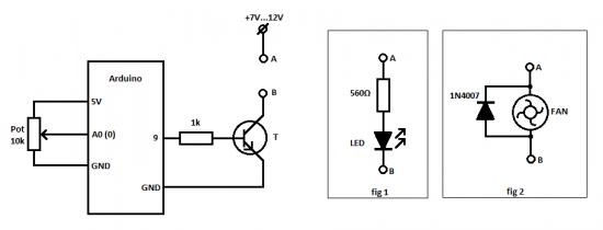
The LED Brightness or Fan Speed with Arduino – Tutorial #7
Published:2013/8/13 21:27:00 Author:lynne | Keyword: The LED Brightness or Fan Speed with Arduino , Tutorial #7
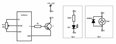
We set the potentiometer pin as 0 (A0 on the Arduino Uno board), the CONTROL variable is the voltage that is used to cotrol the led brightness of the speed of the fan. In the setup() function the CONTROL pin 9 is set as OUTPUT. In the loop() we are getting the analog reading value of the voltage that is applied on pin A0 or 0.
Then use the map() function to translate the value 1024 to 255 and store it in the value variable. After that Arduino writes this value to the CONTROL pin, resulting in a variable voltage that is dependent on the pontetiometer value (its voltage on the adjustable pin, in this case it is connected as a voltage divider *see the schematic).
 (View)
View full Circuit Diagram | Comments | Reading(1320)
Up/Down Fading LED
Published:2013/7/29 1:51:00 Author:lynne | Keyword: Up/Down Fading LED
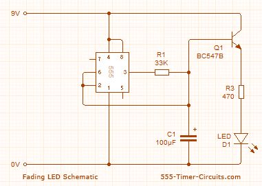
These two circuits make a LED fade on and off. The first circuit charges a 100u and the transistor amplifies the current entering the 100u and delivers 100 times this value to the LED via the collector-emitter pins. The circuit needs 9v for operation since pin 2 of the 555 detects 2/3 Vcc before changing the state of the output so we only have a maximum of 5.5v via a 470R resistor to illuminate the LED. (View)
View full Circuit Diagram | Comments | Reading(2117)
Headlight Flasher
Published:2013/7/25 21:02:00 Author:muriel | Keyword: Headlight Flasher
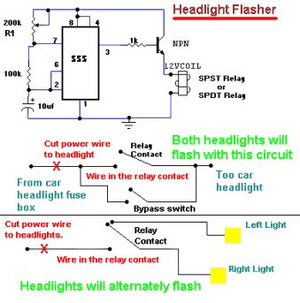
+September 98 Project : Headlight FlasherThis circuit was requested from an email. It will allow your car headlights to flash on and off at the same time or it will cause them to flash alternately. The circuit is based on the 555 timer. It is used in the astable mode. The 555 timer output will go high for an adjustable period of time and then turn off. It will then repeat the procedure.The time is adjusted by R1. To hook up the circuit to your car you must locate the positive wire from the fuse box to the headlights. Cut the wire and insert the relay contact and bypass switch. The bypass switch will allow you to bypass the relay contact for normal headlight operation. In the alternateing headlight configuration you must cut the positive wire to each headlight and wire in the relay contact. (View)
View full Circuit Diagram | Comments | Reading(0)
Pulsing Third Brake Lights
Published:2013/7/25 21:00:00 Author:muriel | Keyword: Pulsing Third Brake Lights

PartsIC1,IC2 = 555 Timer, RS #276-1723SCR1 = NTE/ECG5402, RS #276-1067, EC103A, MCR104, etc.Q1 = NTE/ECG197, SK3083, TIP125, or equivalentD1,D2,D3 = 1N4148, 1N914, NTE/ECG519, RS #276-1122D4,D5 = 1N5400, NTE/ECG5850, RS #276-1141, or equivalentR1 = 18KR2 = 330 ohm (RS #271-1315)R3 = 270KR4 = 82KR5,R6 = 1K2R8 = 100 ohm (RS# 271-1311)P1 = 50K, 10-turnP2 = 10K, 10-turnC1 = 100µF/16V (RS# 272-1016)C2 = 22µF/16V (RS# 272-1014)C3 = 220µF/16V (RS# 272-1017)C4 = 10µF/16V (RS# 272-1013)Q1 is a PNP Silicon Audio Power Out/Medium Power Switch Transistor, 7A, with a TO-220 case. As long as you have a transistor which is close it will work fine. The SCR is a 100vrm, 0.8A, sensitive gate with a TO-92 case. Diodes D1, D2 and D3 are standard small signal diodes. Power diodes D4 and D5 are the 6A, 50prv types, cathode case. The 60vrm type will work as well. I used for IC1 & IC2 the LM555 type. P1 controls the 'on' and pulse-duration, P2 controls the pulse-timing.
Applying the Brakes: When you first press the brakes, this circuit will turn on your 3rd brake light via the main brake lights. After about a second a series of short strobe pulses occur. The number of pulses range from approximately 1 to 10, depending on the setting of P1/P2 and when the brake pedal was applied last. After the pulses have been applied the third brake light assumes normal operation. The prototype was set for five flashes which seemed more than enough. Two days later I re-adjusted the trimmer potentiometers for 4 flashes--1/2 second pause--4 flashes. Looks pretty cool!
Circuit Description:The schematic consists of two 555 timer/oscillators in a dual timer configuration both setup in astable mode. When power is applied via the brake pedal, the brake light driver Q1 is switched on via the low-output pin 3 of IC2, and timer IC1 begins its timing cycle. With the output on pin 3 going high, inhibiting IC2's pin 2 (trigger) via D2, charge current begins to move through R3, R4 and C2.When IC1's output goes low, the inhibiting bias on pin 2 of IC2 is removed and IC2 begins to oscillate, pulsing the third brake light via the emitter of Q1, at the rate determined by P2, R6, and C4. That oscillation continues until the gate-threshold voltage of SCR1 is reached, causing it to fire and pull IC1's trigger (pin 2) low. With its trigger low, IC1's ouput is forced high, disabling IC2's trigger. With triggering disabled, IC2's output switches to a low state, which makes Q1 conduct turning on the 3rd Brake Light until the brakes are released. Obviously, removing the power from the circuit at any time will reset the Silicon Controlled Rectifier SCR1, but the RC network consisting of R4 and C2 will not discharge immediately and will trigger SCR1 earlier. So, frequent brake use means fewer flashes or no flashes at all. But I think that's okay. You already have the attention from the driver behind you when you used your brakes seconds before that.The collector/emitter voltage drop accross Q1 together with the loss over the series fed diodes D4/D5, will reduce the maximum available light output, but if your car's electrical system is functioning normally in the 13 - 14volt range, these losses are not noticeable.
Building Tips: You can easily build this circuit on perfboard or on one of RS/Tandy's experimentors boards (#276-150), or use the associated printed circuit board listed here.Keep in mind that Q1 will draw most likely 2 or 3 amps and mounting this device on a heat sink is highly recommended. Verify that the scr is the 'sensitive gate' type. In incandecent bulbs, there is a time lag between the introduction of current and peak brightness. The lag is quite noticeable in an automotive bulb, so the duration of a squarewave driving such a bulb should be set long enough to permit full illumination. For that reason, and because lamps and car electrical systems vary, adjustment via P1 and P2 is necessary to provide the most effective pulse timing for your particular vehicle.The reason that the third light is connected to both brake lights is to eliminate the possibility of a very confusing display when you use your turn signal with the brakes applied.The cathode of D4 and D5 are tied together and go to point 'B' of the third brake light in the component layout diagram. Point 'A' goes to the other leg of the third brake light. Most if not all third brake lights in Canada & USA have two wires, the metal ones also have a ground wire which obviously goes to ground. I don't know the wiring schema for Australian and European third brake lights.Don't forget the three jumpers on the pcb; two jumpers underneath IC1/IC2 between pin 4/8 and the one near Q1/R6.If you use a metal case, don't forget to insulate the D4/D5 diodes.Some 90's cars, like my 1992 Mercury Sable, have two bulbs inside the third brake light, each bulb is hooked up seperately to the left and right brake light for reasons only Ford knows. Click here for a possible 2-bulb hookup. It shows how I modified mine to get it working; and that was easier than I expected. Current draw with the two bulbs was measured at 1.85Amps (1850mA). Even with double the current none of the circuit components were getting hot. I had to re-adjust the two pots to make it flash since the bench testing was done with one bulb.
Bench Testing:I tested different semiconductors like the 1N5401/1N5404, NTE153, and 4A type powerdiodes for D4/D5. All worked very well. As expected, Q1 is getting very hot. Current draw was measured between 680 - 735mA with a regular automotive 'headlight' bulb, extra heavy duty to make sure the circuit was safe. I tested several other power transistors including some darlingtons like the TIP125 and the TIP147. I eventually settled for the TIP125 myself because I had it available but any thing with 5A or more will do fine.The actual third brake bulb is a lot smaller. Adjusting the trimpots (P1/P2) may take a bit of patience but really fine-tunes the circuit well. The only drawback of this circuit is the discharge lag coming from the electrolytic capacitor C2 and the R4 resistor. Especially if the brakes are used often or at short intervals the third brake light will not flash or maybe flash once or twice. Again, this is because the R-C combo does not have enough time to discharge in between braking. It takes about 12 seconds to discharge C2. (View)
View full Circuit Diagram | Comments | Reading(1692)
Phone Light Flasher
Published:2013/7/25 20:57:00 Author:muriel | Keyword: Phone Light Flasher
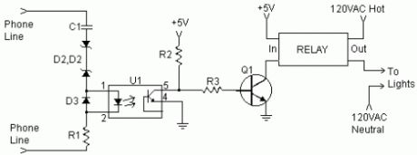
Parts:C1 0.47uF 250V CapacitorR1, R2 10K 1/4 W ResistorR3 1K 1/4W ResistorD1, D2 20V 1/4W Zener DiodeD3 1N4148 DiodeQ1 2N3904 NPN Transistor or 2N2222U1 4N27 Opto IsolatorRELAY Solid State Or Regular Relay (See Notes)MISC Case, Wire, Board
Notes:1. You may need to use a lower voltage zener for D1 and D2.2. You can use a regular relay instead of a solid state relay, but the arcing accross the contacts may destroy it pretty quickly.3. Be very sure that you have not accidentally connected 120V to the phone line when building and installing this circuit. (View)
View full Circuit Diagram | Comments | Reading(1161)
The flashing Heart
Published:2013/7/23 21:12:00 Author:muriel | Keyword: The flashing Heart

The Circuit Diagram is shown in Figure 1. It consists of a 4047 low-power monostable/astable multivibrator, IC1, used in the astable mode to provide the timing pulses to control the flash rate of the LEDs. To accomplish the astable mode, pins 4, 5, 6, and 14 are connected to +12VDC and pins 7, 8, 9, and 12 are connected to ground. Pins 1 and 3 are connected to C2 and pins 2 and 3 are connected to potentiometer R9. A fixed value resistor can be used in place of the potentiometer R9, if the flash rate does not need to be adjusted. These three pins make up the R-C timing circuit. The output pulses from the 4047 are taken from pins 10, 11, and 13. Pin 10 is the Q output and pin 11 is the Q-not output. These two pins are onnected to R6 and R7 respectively.
The collectors of Q2 and Q3 are connected to R4 and R5 respectively, which are connected to the cathodes of the Yellow LEDs. Pin 13 is the oscillator output and is connected to R8, which is connected to the base of Q1. The collector of Q1 is connected to R3, which is connected to the cathodes of the Red LED's. The emitters of the three transistors are connected to ground. The Green LEDs are connected to R1 and R2, which are connected to +12VDC. Resistors R1-R8 are current limiting resistors and the correct wattage for these resistors should be used to prevent excessive heat. The resistive values may be changed to vary the brightness of the LEDs. The circuit is powered by PS1, a wall transformer, which is connected to a filter capacitor C1. It must be between 10 to 15 VDC and at least 500mA.
ConstructionProbably the most difficult part of this project is making the printed circuit board, Figure 2. The board used in the prototype took several hours to make using dry transfers. Using a different technique, such as photo resist, may be faster for the experienced hobbyist. Once the board is etched and drilled, the jumper wires should be placed on the board and soldered, as shown on Figure 3. Next the 84 Yellow LEDs should be placed around the border of the board, followed by the 42 Red LEDs that make up the heart and then the 16 Green LEDs that make up the letters I and U. Resistors R1-R9 and capacitors C1and C2 should be placed on the board next and then the power supply, PS1. Sockets were used in the prototype for the I.C. and transistors. A socket for the I.C. is required, but the sockets for the transistors are not. Special care should be taken when handling the CMOS I.C., as a static discharge will destroy it. When you are finished soldering, check the board over for mistakes. If everything looks okay, apply power. (View)
View full Circuit Diagram | Comments | Reading(1286)
Fading LED
Published:2013/7/23 21:09:00 Author:muriel | Keyword: Fading LED
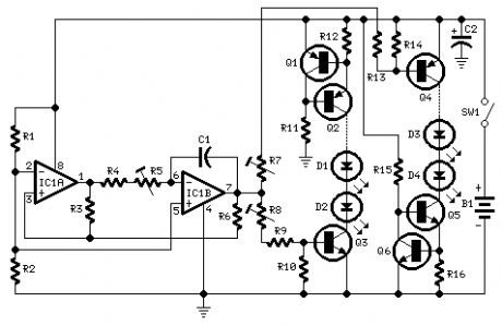
Parts:R1,R2 4K7 1/4W ResistorsR3 22K 1/4W ResistorR4 1M 1/4W Resistor (See Notes)R5 2M2 1/4W Carbon Trimmer (See Notes)R6,R10,R11,R14,R15 10K 1/4W ResistorsR7,R8 47K 1/4W Carbon Trimmers (See Notes)R9,R13 27K 1/4W ResistorsR12,R16 56R 1/4W ResistorsC1 1µF 63V Polyester CapacitorC2 100µF 25V Electrolytic CapacitorD1-D4 etc 5 or 3mm. LEDs (any type and color) (See Notes)IC1 LM358 Low Power Dual Op-ampQ1,Q2,Q4 BC327 45V 800mA PNP TransistorsQ3,Q5,Q6 BC337 45V 800mA NPN TransistorsSW1 SPST miniature Slider SwitchB1 9V PP3 BatteryClip for PP3 Battery
Device purpose:This circuit operates two LED strips in pulsing mode, i.e. one LED strip goes from off state, lights up gradually, then dims gradually, etc. while the other LED strip do the contrary.Each strip can be made up from 2 to 5 LEDs at 9V supply.
Circuit operation:The two Op-Amps contained into IC1 form a triangular wave generator. The rising and falling voltage obtained at pin #7 of IC1 drives two complementary circuits formed by a 10mA constant current source (Q1, Q2 and Q5, Q6) and driver transistor (Q3 and Q6).R4, R5 & C1 are the timing components: the total period can be varied changing their values. R7 & R8 vary the LEDs brightness.
Notes:For those whishing to avoid the use of trimmers, suggested values for a 9V supply are:R4=3M9, R9 & R13=47K and trimmers replaced by a short.Whishing to use a wall-plug transformer-supply instead of a 9V battery, you can supply the circuit at 12V, allowing the use of up to 6 LEDs per strip, or at 15V, allowing the use of up to 7 LEDs per strip.In this case, the value of the trimmers R7 & R8 should be changed to 100K.
(View)
View full Circuit Diagram | Comments | Reading(1338)
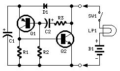
LEDs or Lamps Sequencer
Published:2013/7/23 21:08:00 Author:muriel | Keyword: LEDs, Lamps, Sequencer
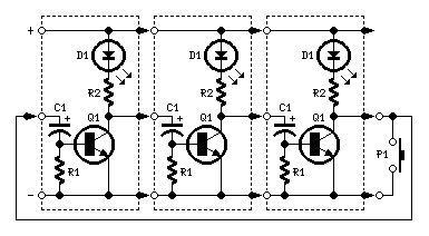

Parts:R1 1K5 1/4W ResistorR2 680R 1/4W Resistor (Optional, see text)C1 47µF 25V Electrolytic CapacitorD1 LED any typeQ1 BC337 45V 800mA NPN TransistorP1 SPST PushbuttonLP1 Filament Lamp 12 or 24V (See text)
Comments:The purpose of this circuit was to create a ring in which LEDs or Lamps illuminate sequentially. Its main feature is a high versatility: you can build a loop containing any number of LEDs or Lamps, as each illuminating device has its own small circuit.The diagrams show three-stage circuits for simplicity: you can add an unlimited number of stages (shown in dashed boxes), provided the last stage output was returned to the first stage input, as shown.P1 pushbutton purpose is to allow a sure start of the sequence at power-on but, when a high number of stages is used, it also allows illumination of more than one LED or Lamp at a time, e.g. one device illuminated and three out and so on.After power-on, P1 should be held closed until only the LED or Lamp related to the module to which the pushbutton is connected remains steady illuminated. When P1 is released the sequencer starts: if P1 is pushed briefly after the sequence is started, several types of sequence can be obtained, depending from the total number of stages.
Notes:If one LED per module is used, voltage supply can range from 6 to 15V.You can use several LEDs per module. They must be wired in series and supply voltage must be related to their number.Using 24V supply (the maximum permitted voltage), about 10 LEDs wired in series can be connected to each module, about 7 at 15V and no more than 5 at 12V.The right number of LEDs can vary, as it is depending by their color and brightness required.Using lamps, voltage supply can range from 9 to 24V. Obviously, lamp voltage must be the same of supply voltage.In any case, lamps may also be wired in series, e.g. four 6V lamps wired in series can be connected to each module and powered by 24V supply.If you intend to use lamps drawing more than 400mA current, BC337 transistors should be substituted by Darlington types like BD677, BD679, BD681, 2N6037, 2N6038, 2N6039 etc.As Darlington transistor usually have a built-in Base-Emitter resistor, R1 may be omitted, further reducing parts counting.Sequencer speed can be varied changing C1 value.A similar design appeared in print about forty years ago. It used germanium transistors and low voltage lamps. I think the use of LEDs, silicon transistors, Darlington transistors and 24V supply an interesting improvement. (View)
View full Circuit Diagram | Comments | Reading(1440)
Bicycle back Safety Lights
Published:2013/7/23 21:05:00 Author:muriel | Keyword: Bicycle back, Safety Lights
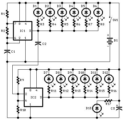
Parts:R1 10K 1/4W ResistorR2,R9,R10 100K 1/4W ResistorsR3-R8,R11-R16 10R 1/4W ResistorsR17 150R 1/4W ResistorC1 1µF 63V Polyester CapacitorC2 10nF 63V Polyester CapacitorC3 100µF 25V Electrolytic CapacitorD1-D13 Red LEDs 5mm. or bigger, high efficiencyIC1,IC2 7555 or TS555CN CMos Timer ICSW1 SPST Slider SwitchB1 3V Battery (2 AA 1.5V Cells in series)
Device purpose:This circuit has been designed to provide a clearly visible light, formed by 13 high efficiency flashing LEDs arranged in a pseudo-rotating order. Due to low voltage, low drain battery operation and small size, the device is suitable for mounting on bicycles as a back light, or to put on by jogger/walkers.
Circuit operation:IC1 is a CMos version of the 555 IC wired as an astable multivibrator generating a 50% duty-cycle square wave at approx. 4Hz frequency. At 3V supply, 555 output (pin 3) sinking current operation is far better than sourcing, then LED D1-D6 are connected to positive supply. In order to obtain an alternate flashing operation, a second 555 IC is provided, acting as a trigger plus inverter and driving LEDs D7-D12. D13 is permanently on.The LEDs are arranged in a two series display as shown below, with a center LED permanently on. This arrangement and the alternate flashing of the two series of LEDs provide a pseudo-rotating appearance.
(View)
View full Circuit Diagram | Comments | Reading(1141)
Two-wire Lamp Flashers
Published:2013/7/23 21:04:00 Author:muriel | Keyword: Two-wire, Lamp Flashers
Parts:R1 6K8 1/4W ResistorR2 270K 1/4W ResistorR3 22K 1/4W ResistorC1 220µF 25V Electrolytic CapacitorC2 10µF 25V Electrolytic CapacitorD1 1N4002 100V 1A DiodeQ1 BC557 45V 100mA PNP TransistorQ2 BD139 80V 1.5A NPN TransistorLP1 Existing filament Lamp: any type in the range 3-24V 10W max.SW1 Existing On-Off switchB1 Existing V DC source: any type in the range 3-24Vsuited to the lamp adopted
Device purpose:This circuit has been designed to provide that continuous light lamps already wired into a circuit, become flashing. Simply insert the circuit between existing lamp and negative supply.Especially suited for car or panel pilot lights, this device can drive lamps up to 10W.
Notes:Break lamp(s) to negative supply connection(s), then insert the circuit between existing lamp(s) connection(s) and negative supply (respecting polarities!).C1 value can be varied from 100 to 1000µF or higher, in order to change flashing frequency.Although rather oversized, this circuit can also drive any LED, providing a suitable resistor is fitted in series with the light emitting device.The resistor should be in the range 47R to 2K2, depending on supply voltage
(View)
View full Circuit Diagram | Comments | Reading(1337)
Lamp Pulser
Published:2013/7/23 21:03:00 Author:muriel | Keyword: Lamp Pulser
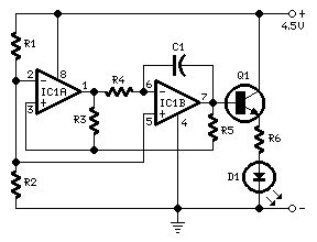
Parts:R1,R2 4K7 1/4W ResistorsR3 22K 1/4W ResistorR4 2M2 1/4W Resistor (See Notes)R5 10K 1/4W ResistorR6 47R 1/4W Resistor (See Notes)C1 1µF 63V Polyester CapacitorD1 5mm. Red LED (See Notes)IC1 LM358 Low Power Dual Op-ampQ1 BC337 45V 800mA NPN Transistor
Circuit operation:This circuit operates a LED in pulsing mode, i.e. the LED goes from off state, lights up gradually, then dims gradually, etc.This operation mode is obtained by a triangular wave generator formed by two op-amps contained in a very cheap 8 pin DIL case IC. Q1 ensures current buffering, in order to obtain a better load drive.R4 & C1 are the timing components: using the values shown in the parts list, the total period is about 4 seconds.
Notes:The most satisfying results are obtained adopting for R4 a value ranging from 220K to 4M7.Adopting for R4 a value below 220K, the pulsing effect will be indistinguishable from a normal blinking effect.The LED can be any type and color.You can use a filament lamp instead, provided its features are comprised in the range 3.2 to 6V, 200mA max.Using a lamp as a load, R6 must be omitted.Voltage supply range can be 4 to 6V: 4.5V is the best compromise.Don't supply the circuit with voltages exceeding 6V: it will work less good and Q1 could be damaged when a lamp was used as the load.At 6V supply, increase R6 value to 100 Ohm. (View)
View full Circuit Diagram | Comments | Reading(1290)
Dancing LED
Published:2013/7/22 20:15:00 Author:muriel | Keyword: Dancing LED
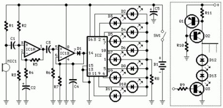
Parts:R1 10K 1/4W ResistorR2,R3 47K 1/4W ResistorsR4 1K 1/4W ResistorR5,R6,R7 100K 1/4W ResistorsR8 820R 1/4W ResistorC1,C3 100nF 63V Ceramic or Polyester CapacitorsC2 10µF 50V Electrolytic CapacitorC4 330nF 63V Polyester Capacitor (See Notes)C5 100µF 25V Electrolytic CapacitorD1 1N4148 75V 150mA DiodeD2-D11 5 or 3mm. LEDs (any type and color)IC1 LM358 Low Power Dual Op-ampIC2 4017 Decade counter with 10 decoded outputs ICM1 Miniature electret microphoneSW1 SPST miniature Slider SwitchB1 9V PP3 BatteryClip for PP3 BatteryAdditional circuit parts (see Notes):R9,R10 10K 1/4W ResistorsR11 56R 1/4W ResistorD12,D13 etc 5 or 3mm. LEDs (any type and color)Q1,Q2 BC327 45V 800mA PNP TransistorsQ3 BC337 45V 800mA NPN Transistor
Device purpose:The basic circuit illuminates up to ten LEDs in sequence, following the rhythm of music or speech picked-up by a small microphone. The expanded version can drive up to ten strips, formed by up to five LEDs each, at 9V supply.
Circuit operation:IC1A amplifies about 100 times the audio signal picked-up by the microphone and drives IC1B acting as peak-voltage detector. Its output peaks are synchronous with the peaks of the input signal and clock IC2, a ring decade counter capable of driving up to ten LEDs in sequence.An additional circuit allows the driving of up to ten strips, made up by five LEDs each (max.), at 9V supply. It is formed by a 10mA constant current source (Q1 & Q2) common to all LED strips and by a switching transistor (Q3), driving a strip obtained from 2 to 5 series-connected LEDs. Therefore one transistor and its Base resistor are required to drive each strip used.
Notes:The sensitivity of the circuit can be varied changing R4 value.C4 value can be varied from 220 to 470nF in order to change the circuit speed-response to music peaks.Adopting the additional circuit, only one item for R10, R11, Q1 and Q2 is required to drive up to ten LED strips. On the contrary, one item of R9 and Q3 is necessary to drive each strip you decided to use.Each R9 input must be connected to IC2 output pins, in place of the LEDs D2-D11 shown. R8 must also be omitted.Whishing to use a lower number of LEDs or LED strips, pin #15 of IC2 must be disconnected from ground and connected to the first unused output pin. Example:if you decided to use 5 LEDs, pin #15 of IC2 must be connected to pin #1; if you decided to use 8 LEDs, pin #15 of IC2 must be connected to pin #9 etc.Current drawing of the circuit is about 10mA.Whishing to use a wall-plug transformer-supply instead of a 9V battery, you can supply the circuit at 12V, allowing the use of up to 6 LEDs per strip, or at 15V, allowing the use of up to 7 LEDs per strip.
(View)
View full Circuit Diagram | Comments | Reading(1382)
Triple Stroboscope
Published:2013/7/22 20:14:00 Author:muriel | Keyword: Triple Stroboscope
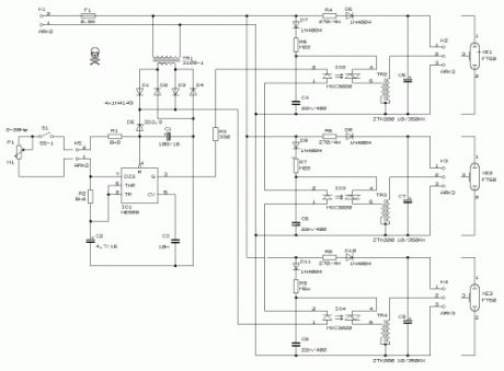
This circuit enables observation of movement between other stroboscopes. Generation of rectangular signal is based on NE555. This circuit requires a low power supply that is made from a simple transformer TR1, traditional rectifier bridge and zener diode.NE555 works in multivibrator mode generating astable pulses of 2Hz to 20Hz.The frequency is adjusted by potentiometer P1. The control potentiometer P1 can be placed as far as 30 meters away, for suspension of stroboscope’s work from far away.It is east to find all parts with facility in every electronic store, but it may be difficult to find the transformers TR2, TR3, TR4.Take extreme care handling this circuit because near C5-C7-C9 high voltages are present.
PartsR1 = 6,8 kR2 = 5,6 kR3 = 330R4,R6,R8 = 270 / 5 WR5,R7,R9 = 220 kP1 = 100 k linear potentiometerC1 = 100 uF / 16 VC2 = 4,7 uF / 16 VC3 = 10 nFC4,C6,C8 = 22 nF / 400 V, MKSC5,C7,C9 = 10 uF / 350 V, electrolytic (high quality)TR1 = Ordinary transformer 230 V / 9 V, 1,5 VATR2,TR3,TR4 = stroboscope transformer np (ZTK200)D1,D2,D3,D4 = 1N4149D5 = BZX85V Zener 3.9D6,D7,D8,D9,D10,D11 = 1N4004IO1 = NE555IO2,IO3,IO4 = MOC3020XE1,XE2,XE3 = stroboscope lamps FT50F1 = Fuse 0.8 A, 20 mmK1,K5 = connectors ARK200-2K2,K3,K4 = connectors ARK200-3S1 = Switch
(View)
View full Circuit Diagram | Comments | Reading(1356)
Knightrider lights for model cars
Published:2013/7/22 20:13:00 Author:muriel | Keyword: Knightrider lights, model cars
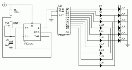
This simple circuit drives 6 LEDs in 'Knightrider scanner mode'. Power consumption depends mainly on the type of LEDs used if you use a 7555 (555 CMOS version).
Note that VDD and GND for the ICs are not shown in the circuit drawing.Pin-outs:(7)555 1 GND 2 TRIGGER 3 OUTPUT 4 RESET 5 CONTROL VOLTAGE 6 THRESHOLD 7 DISCHARGE 8 VDD 40171 Q5 2 Q1 3 Q0 4 Q2 5 Q6 6 Q7 7 Q3 8 GND 9 Q810 Q411 Q912 CO13 NOT ENABLE14 CLK15 RESET16 VDD (View)
View full Circuit Diagram | Comments | Reading(1618)
220 Volts Flashing Lamp
Published:2013/7/22 20:13:00 Author:muriel | Keyword: 220 Volts , Flashing Lamp
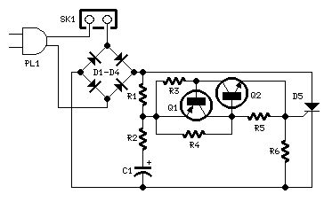
Parts:R1 100K 1/4W ResistorR2,R5 1K 1/4W ResistorsR3,R6 470R 1/4W ResistorsR4 12K 1/4W ResistorC1 1000µF 25V Electrolytic CapacitorD1-D4 1N4007 1000V 1A DiodesD5 P0102D 400V 800mA SCRQ1 BC327 45V 800mA PNP TransistorQ2 BC337 45V 800mA NPN TransistorPL1 Male Mains plugSK1 Female Mains socket
Device purpose:This circuit is intended as a reliable replacement to thermally-activated switches used for Christmas tree lamp-flashing. The device formed by Q1, Q2 and related resistors triggers the SCR. Timing is provided by R1,R2 & C1. To change flashing frequency don't modify R1 and R2 values: set C1 value from 100 to 2200µF instead.Best performances are obtained with C1=470 or 1000µF and R4=12K or 10K. Due to low consumption of normal 10 or 20 lamp series-loops intended for Christmas trees (60mA @ 220V typical for a 20 lamp series-loop), very small and cheap SCR devices can be used, e.g. C106D1 (400V 3.2A) or TICP106D (400V 2A), this last and the suggested P0102D devices having TO92 case.
Important Note:For proper operation it's absolutely necessary to employ high Gate-sensitive SCRs.If you are unable to find these devices you can use Triacs instead. In this case the circuit operates also with relatively powerful devices. A recommended Triac type is the ubiquitous TIC206M (600V 4A) but many others can work.Note that in spite of the Triac, diode bridge D1-D4 is in any case necessary.
This circuit was awarded with publication in ELECTRONICS WORLD Circuit Ideas , June 2000 issue, page 458
(View)
View full Circuit Diagram | Comments | Reading(1394)
Battery-powered Night Lamp 1
Published:2013/7/22 20:12:00 Author:muriel | Keyword: Battery-powered , Night Lamp
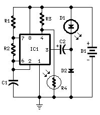
Parts:R1,R2 1M 1/4W ResistorsR3 47K 1/4W Resistor (optional: see Notes)R4 Photo resistor (any type, optional: see Notes)C1 100nF 63V Polyester CapacitorC2 220µF 25V Electrolytic CapacitorD1 LED Red 10mm. Ultra-bright (see Notes)D2 1N5819 40V 1A Schottky-barrier Diode (see Notes)IC1 7555 or TS555CN CMos Timer ICB1 1.5V Battery (AA or AAA cell etc.)
Device purpose:This circuit is usable as a Night Lamp when a wall mains socket is not available to plug-in an ever running small neon lamp device. In order to ensure minimum battery consumption, one 1.5V cell is used, and a simple voltage doubler drives a pulsating ultra-bright LED: current drawing is less than 500µA.An optional Photo resistor switches-off the circuit in daylight or when room lamps illuminate, allowing further current economy.This device will run for about 3 months continuously on an ordinary AA sized cell or for around 6 months on an alkaline type cell but, adding the Photo resistor circuitry, running time will be doubled or, very likely, triplicated.
Circuit operation:IC1 generates a square wave at about 4Hz frequency. C2 & D2 form a voltage doubler, necessary to raise the battery voltage to a peak value able to drive the LED.
Notes:IC1 must be a CMos type: only these devices can safely operate at 1.5V supply or less.If you are not needing Photo resistor operation, omit R3 & R4 and connect pin 4 of IC1 to positive supply.Ordinary LEDs can be used, but light intensity will be poor.An ordinary 1N4148 type diode can be used instead of the 1N5819 Schottky-barrier type diode, but LED intensity will be reduced due to the higher voltage drop.Any Schottky-barrier type diode can be used in place of the 1N5819.
(View)
View full Circuit Diagram | Comments | Reading(1065)
Adjustable Strobe Lights
Published:2013/7/22 20:11:00 Author:muriel | Keyword: Adjustable Strobe Lights
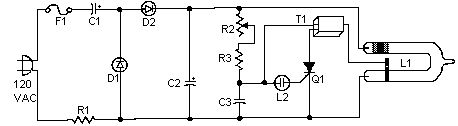
This one uses a much more powerful horse shoe Xenon tube which produces more light. You can also control the flash rate up to about 20Hz. Do not look directly at the flash tube when this thing is on!
PartsR1 250 Ohm 10 Watt ResistorR2 500K PotR3 680K 1/4 Watt ResistorD1,D2 1N4004 Silicon DiodeC1, C2 22 uF 350V CapacitorC3 0.47uF 400 Volt Mylar CapacitorT1 4KV Trigger Transformer (see Notes )L1 Flash Tube (see Notes )L2 Neon BulbQ1 106 SCRF1 115V 1A FuseMisc Case, Wire, Line Cord, Knob For R2Notes1. T1 and L1 are available from The Electronics Goldmine2. This ciruits is NOT isolated from ground. Use caution when operating without a case. A case is required for normal operation. Do not touch any part of the circuit with the case open or not installed.3. Most any diodes rated at greater then 250 volts at 1 amp can be used instead of the 1N4004's.4. Do not operate this circuit at high flash rates for more than about 30 seconds or else C1 and C2 will overheat and explode.5. There is no on/off switch in the schematic, but you can of course add one. (View)
View full Circuit Diagram | Comments | Reading(1383)
Nite Rider Lights
Published:2013/7/22 20:10:00 Author:muriel | Keyword: Nite Rider Lights

As a keen cyclist I am always looking for ways to be seen at night. I wanted something that was a novelty and would catch the motorists eye. So looking around at my fellow cyclists rear lights, I came up with the idea of 'NITE-RIDER'. NINE extra bright LED's running from left to right and right to left continuously. It could be constructed with red LEDs for use on the rear of the bike or white LED's for an extra eye catcher on the front of the bike.All IC's are CMOS devices so that a 9V PP3 battery can be used, and the current drawn is very low so that it will last as long as possible.
Parts1 555 timer IC4.1 4027 flip flop IC1.2 4017 Decade Counter IC2 and IC3.3 4071 OR gate IC5, IC6 and IC7.1 470 Ohm resistor 1/4 watt R3.2 10K resistors 1/4 watt R1 and R2.1 6.8UF Capasitor 16V C1.9 Super brght LED's 1 to 9.1 9V PP3 Battery.1 single pole switch SW1.1 Box.
How The Circuit Works.IC4, C1, R1 and R2 are used for the clock pulse which is fed to both the counters IC2 and IC3 Pin 14.IC1 is a Flip Flop and is used as a switch to enable ether IC2 or IC3 at pin 13.IC7a detects when ether IC2 or IC3 has reached Q9 of the counter pin 11.IC5, IC6 and IC7a protects the outputs of the counters IC2 and IC3 using OR gates which is then fed to the Anodes of theLED's 1 to 9.
(View)
View full Circuit Diagram | Comments | Reading(1397)
LED Chaser 1
Published:2013/7/22 20:10:00 Author:muriel | Keyword: LED Chaser
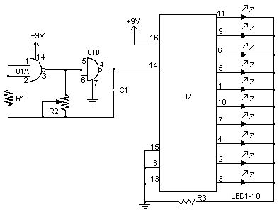
I don't know why, but people like blinking lights. You see LED chasers everywhere, in TV shows (Knight Rider), movies, and store windows. This schematic is my version of a simple 10 LED chaser. There is no 555 timer used because at my local electronics store they are over $4 Cdn. Instead, an oscillator made up of two sections of a 4011 NAND gate is employed. This chip is very inexpensive and extremely common.
Parts:R1 1 Meg 1/4W ResistorR2 100K PotR3 1K 1/4W Resistor or 220Ohm if using blue LEDsC1 0.1uF 16V Ceramic Disk CapacitorU1 4011 CMOS NAND GateU2 4017 CMOS CounterLED1-10 LEDs Of Any ColourMISC Board, Sockets For ICs, Knob For R2
Notes:1. Use R2 to adjust the chase rate .2. You may need to use a lower value resistor if you wish to use blue LEDs. Try 220 Ohm.3. You can also use incandescent lamps instead of LEDs. Use transistors to drive them by connecting the base of the transistors to each of the outputs of the 4017 through a 1K resistor. Connect one end of the lamp to the positive supply. Then connect the other end to the collector of the transistor. The emitter then goes to ground. Depending on the lamps, you may need power transistors that are heat sinked.4. C1 may be replaced with a larger value for a slower chase rate .5. If you have problems with weird circuit behavior, try replacing R1 with a 33K resistor, and increasing C1 to 1uF.6. If you plan to use this circuit in your car, be warned that in some areas it is illegal to have red, blue or yellow flashing lights unless you are an emergency vehicle. (View)
View full Circuit Diagram | Comments | Reading(1326)
6V Ultra-Bright LED Chaser
Published:2013/7/22 20:09:00 Author:muriel | Keyword: 6V, Ultra-Bright, LED, Chaser

GeneralThis is a spectacular but completely useless project. It lights Ultra-Bright LEDs in a sequence and each LED flashes brightly very briefly. The LEDs light-up going around and around since they are mounted in a circle (on a CD), then they pause before chasing again. The very brief flash of each LED (15ms) and the pauses (1 second) reduce the average current so the battery should last a long time.For user convenience, this project has a stepper speed control and a brightness control. At slower speeds and/or reduced brightness, the battery’s life is extended considerably.At full brightness, the LEDs flash extremely brightly. More than one of this project grouped together occasionally synchronize, lighting the whole room for a moment.
OperationAt maximum speed, the LEDs don’t appear to flash, instead they appear to move from one lighted one to the next, around and around. They rotate completely for 4 rotations in two seconds, and then turn off for a one second pause then repeat the sequence. At a lower speed, the number of rotations before the pause is less. It will do three rotations, two or even only one rotation at its slowest speed. A sequence of rotations starts with LED #2 and end with LED #9.
SpecificationsBattery: Four AA alkaline cells.Battery life:Minimum speed and brightness 2.3 yearsMedium speed and brightness 1 yearMinimum speed, maximum brightness 4.1 monthsMaximum speed and brightness 3.8 weeksBrightness: controlled with Pulse width Modulation, from off to extremely bright (4000mcd).Stepper speed: 2 LEDs/sec to 2 revolutions/sec.Pulse Width Modulation frequency: 3.9KHz.LED current: 24mA pulses.LED voltage drop: 3.2V at 24mA. Blue, green and white Ultra-Bright LEDs are suitable.Minimum battery voltage:3V, oscillators do not run.3V, LEDs are very dim.4V, LEDs reach almost full brightness.Radio interference: none.
Circuit DescriptionThe CD74HC4017N high-speed Cmos IC is rated for a maximum supply voltage of 7V. It is rated for a maximum continuous output current of 25mA. In this project, the maximum supply voltage is 6.4V with brand new battery cells and the 24mA output current is so brief that the IC runs cool.The MC14584BCP* IC (Motorola) is an ordinary “4XXX series†3V to 18V Cmos IC, with a very low operating current and low output current. Its extremely high input resistance allows this project to use high value resistors for its timers and oscillators, for low supply current. Its 6 inverters are Schmitt triggers for simple oscillators and very quick switching.IC2 is a 10 stage Johnson counter/decoder. On the rising edge of each clock pulse its outputs step one-at-a-time in sequence. It drives the anode of each conducting LED toward the positive supply.IC1 pins 1 and 2 is a Schmitt trigger oscillator with C3 and C4 paralleled for a very low frequency. R1 and R2 control its frequency and the diodes with R3 combine with the capacitors to produce the 15mS on time for the LEDs.IC1 pins 5 and 6 is the brightness Pulse Width Modulation oscillator. The pot R7 with the associated diodes and resistors allow it to change the duty-cycle of its output for PWM brightness control. It drives the transistor.IC1 pins 3 and 4 is an inverter. It takes the low time (LEDs off) from the clock oscillator, inverts it to a high and shuts-off the brightness oscillator through diode D6.IC1 pins 11 and 10 is a sample-and-hold stage. It takes a sample of the pulse driving LED #9 though D3 and R4 and charges C5 in steps. At maximum speed it takes 4 steps for C5 to charge to the Schmitt switching threshold voltage. R5 and D5 slowly discharge C5 for the pause time.IC1 pins 13 and 12 is an inverter that resets the counter/decoder and shuts-off the clock oscillator through D4, during the pause time.IC1 pins 9 and 8 is not used and is shut-off by grounding its input.T1 is the PWM switching transistor. R9 limits the maximum LED current to 24mA.
ConstructionThe 10 LEDs mount on a Compact-Disc which is glued to a plastic box with contact cement. The box houses the Veroboard circuit in its lower main part with the battery holders on its lid. Multiconductor ribbon cable joins the LEDs to the circuit. The pots mount on the sides of the box.If you turn it down each night, its current is so low an on-off switch isn’t needed.
PartsIC1 MC14584BCP (Motorola) * Ordinary Cmos hex Schmitt trigger invertersIC2 CD74HC4017N High-speed Cmos decade counter/decoderT1 2N3904 or 2N4401 NPN transistorD1 to D8 1N4148 or 1N914 Diodes10 LEDs Blue, green or white Ultra-Bright LEDs with Vf = 3.2V or less at 20mAR1 100K 1/4W resistorR2 1M Linear-taper potentiometerR3 33K 1/4W resistorR4 2.2M 1/4W resistorR5 22M 1/4W resistorR6 47K 1/4W resistorR7 1M Audio-taper (logarithmic) potentiometerR8 1.8K 1/4W resistorR9 68 ohms 1/4W resistorC1 100uF/16V Electrolytic capacitorC2 0.1uF/50V Ceramic capacitorC4 and C4 1uF/63V Metalized poly capacitorC5 470nF Metalized poly capacitorC6 and C7 1nF Metalized poly capacitor
A CD74C14 can also be used for IC1 but R4 = 1M, R5 = 10M, C3 and C5 = 330nF, C4 = 470nF.A 3V LED Chaser project also works well with these changed parts but using a CD74HC14N for IC1.In addition to these changes, R8 = 680 ohms and R9 = 22 ohms. I built one using low-voltage (1.8V at 20mA) orange Ultra-Bright LEDs. The orange one looks good beside the green one.Attachments: 6V LED Ultra-Bright Chaser schematic, Veroboard layout and 3 pictures.I wish I knew how to take a slow picture with my son’s digital camera, so all the LEDs would be lighted, and if I moved it would make nice lighted smears in the picture. (View)
View full Circuit Diagram | Comments | Reading(1577)
| Pages:3/72 1234567891011121314151617181920Under 20 |
Circuit Categories
power supply circuit
Amplifier Circuit
Basic Circuit
LED and Light Circuit
Sensor Circuit
Signal Processing
Electrical Equipment Circuit
Control Circuit
Remote Control Circuit
A/D-D/A Converter Circuit
Audio Circuit
Measuring and Test Circuit
Communication Circuit
Computer-Related Circuit
555 Circuit
Automotive Circuit
Repairing Circuit