
Other Circuit
Index 10
Air-conditioning Circuit Two of Southeast LingShuai Cars
Published:2011/7/7 21:18:00 Author:Michel | Keyword: LingShuai Cars, Air-conditioning Circuit Two
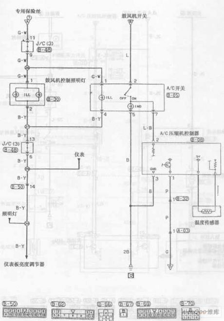
Air-conditioning Circuit of Southeast LingShuai Cars (View)
View full Circuit Diagram | Comments | Reading(604)
White Nosie Generator Circuit of Shift Register and Exclusive-OR Gate
Published:2011/7/9 22:28:00 Author:Michel | Keyword: Shift Register, Exclusive-OR Gate, White Nosie, Generator Circuit
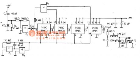
The picture is the white noise generator circuit of shift register and exclusive-or gate.R1 and C1 constitute differential circuit and the circuit enters work state when the switch is turned on.R2, R3 and G3 constitute schmidt trigger circuit.Feet 13 output voltgae of 74HC164(4) is binary signal and the low pass filter composed of L1, C5 and C7 makes amplitude probability density function become normal distribution white noise,namely,Gaussian noise.The cut-off frequency of the low pass filter is enough lower than clock frequency (about 3 MHZ).RP1 is used to adjust and outputs U PWL. (View)
View full Circuit Diagram | Comments | Reading(1788)
Function Generator Circuit of 74HCUO4
Published:2011/7/9 22:44:00 Author:Michel | Keyword: Function Generator Circuit
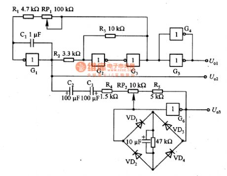
The picture is function generator circuit of 74HCUO4 and G1~G6 is 74HCUO4 inside circuit.This circuit can also output sine wave, rectangular wave and triangle wave at the same time.G1 and C1 constitute Mueller integral circuit and R2, R3, G2 and G3 constitute Schmidt circuit.Output of Schmidt circuit returns to input of miller integral through RP1 and it becomes rectangle wave oscillator. RP1 is used for oscillation frequency adjustment.RP2,R4,R5 and G6 constitute linear inverse amplifier. VD1 ~ VD4 make of diode bridge road and cut top of the triangle wave and turn the triangle wave to sine wave.RP2 adjusts sine wave distortion rate to the minimum value.U.1 outputs rectangle wave,U.2 outputs triangle wave and U.3 outputs sine wave. (View)
View full Circuit Diagram | Comments | Reading(1283)
DS18B20 and 51 Single Chip AT89C2051 Interface Circuit
Published:2011/7/7 22:28:00 Author:Michel | Keyword: 51 Single Chip, Interface Circuit
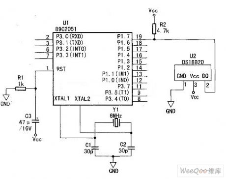
The DS18B20 and 51 single chip AT89C2051 interface circuit is shown as abvoe.The P1.7 mouth line of AT89C2051 is connected to pins 2 data side of DS18820 after being pulled.The pin 1 connects to low power port and pin 3 connects to +5V power supply end. (View)
View full Circuit Diagram | Comments | Reading(2457)
Contrast between SMT Telephone Processing Test Instruments 8960 and CMU200
Published:2011/6/25 8:04:00 Author:Michel | Keyword: Contrast, SMT Telephone, Processing Test Instruments
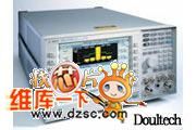
Part No.:8960/E5515CProduction Instructions
It is usedin largeproduction test of mobile phone production processing.
In the mass production of the mobile phone,test throughput and test pass rate are key problems considering of production.Agilent 8960 series 10 wireless communication test device provides the advantageous conditions of taking part in competition immediately for mobile phone producers.The 8960 series 10 test device provides rapid, accurate and repeatable,multiform ability, easy programming and flexible system structure.For phone manufacturers, , it is benificial to reducing test cost and increasing production. (View)
View full Circuit Diagram | Comments | Reading(737)
Automatic Transmission Circuit Eight of Southest Lingshuai Cars
Published:2011/7/7 21:28:00 Author:Michel | Keyword: Lingshuai Cars, Automatic Transmission, Circuit Eight
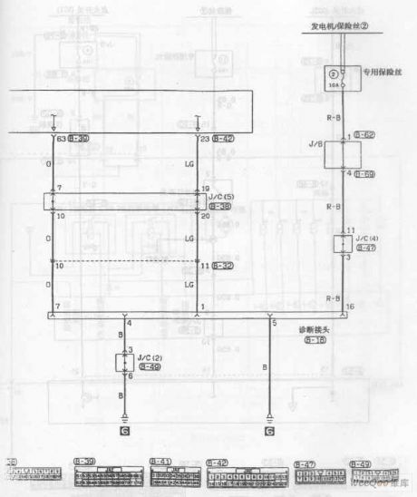
Automatic Transmission Circuit of Southest Lingshuai Cars (View)
View full Circuit Diagram | Comments | Reading(600)
Three-Point Protection Circuit
Published:2011/7/5 5:58:00 Author:Robert | Keyword: Three-Point, Protection
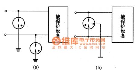
The three-point protection circuit is shown in the picture. When there is a surge voltage flowing into the circuit, the gas discharge tube would guide the surge current to the underground. So that the equipments could get the protective effects.
The picture shows the three-point protection circuit. (View)
View full Circuit Diagram | Comments | Reading(595)
Shuangzhen Dalian Supplies Japan Anti-static Nylon Board
Published:2011/6/24 11:09:00 Author:Michel | Keyword: Shuangzhen Dalian , Japan, Anti-static, Nylon Board
Shuangzhen Dalian supplies Japan Importing anti-static nylon board.Shenzhen Shuangzhen Electronic Co., Ltd is found in Feb. 2007 which has office and warehouses. We are specialied in providing anti-static organic glasses.We devote to providing high-quality industrial products to meet the special needs of high-tech times industry and provide good after-sales service.
Features
MC501CDR6 the filling material of anti-static nylon board is even, anti-static value of all nylon parts are the same.Mechanical processing or after surface wearing, anti-static value has no change. (View)
View full Circuit Diagram | Comments | Reading(593)
Byd MOS Tube Supply
Published:2011/6/24 10:09:00 Author:Michel | Keyword: Byd, MOS Tube, Supply
Detailed Instructions of Byd MOS Tube Supply and Mosfet
Original:BF92N60,BF94N60,BF96N60,BF98N60,BF910N60,BF912N60
Properties and advantages: stable performance and preferential price
Product use: switching power supply, adapters, HID ballast
After-sales service: We provide technical support, and the original BYD signed agreement of the quality.
Packing: tubes (each tube 50 PCS), each box 5000 PCS. The package TO 220 (F)
Note: shenzhen Aisen science and technology is the agent of BYD series
MOS,namely,BF92N60,BF94N60,BF96N60,BF98N60,BF910N60,BF912N60 and we have stocks for long time and welcome to call Mr Zhao via13760184506.In addition,our company is the agent of BYD power management IC-BF1501,AC/AC.
Welcome to download and the information is from www.dzsc.com. (View)
View full Circuit Diagram | Comments | Reading(650)
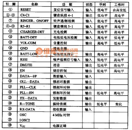
LA7840, LA7841, LA7845 and LA7846-Field scanning output integrated circuit
Published:2011/7/3 2:09:00 Author:leo | Keyword: LA7840, LA7841, LA7845 and LA7846-Field scanning output integrated circuit
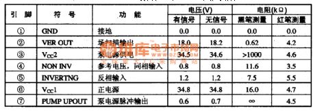
LA7840, LA7841, LA7845 and LA7846 are a kind of field scanning output integrated circuit made by Sanyo Corporation in Japan. They are widely used in color television with different screens.
1.Function features:
They have vertical output circuit, over current protecting circuit and use DC differential input method. The maximum output current of LA7840 is 1.8Ap-p and the maximum output power is 9W. The maximum output current of LA7841 is 2.2Ap-p and the maximum output power is 9W. The maximum output current of LA7845 is 2.2Ap-p and the maximum output power is 11W. The maximum output current of LA7846 is 3Ap-p and the maximum output power is 20W.
2.in functions and related data:
All information about their pin functions and related data are shown in the picture.
(View)
View full Circuit Diagram | Comments | Reading(4668)
TMP87CS38N-XXXX-Projection VT dedicated single chip microcomputer integrated circuit
Published:2011/7/3 2:52:00 Author:leo | Keyword: TMP87CS38N-XXXX-Projection VT dedicated single chip microcomputer integrated circuit
(View)
View full Circuit Diagram | Comments | Reading(647)
Temperature regulation circuit diagram used in valve control
Published:2011/6/18 10:04:00 Author:Nancy | Keyword: temperature regulation, valve control
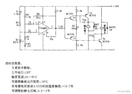
Main technical data:operating voltage: 18Vtemperature range: 25 to 95 ℃sensor maximum allwable temperature: 100 ℃temperature bias under ±10% power supply fluctuation: <0.1°Kadjustable static area: 0.2 to 1°K (View)
View full Circuit Diagram | Comments | Reading(839)
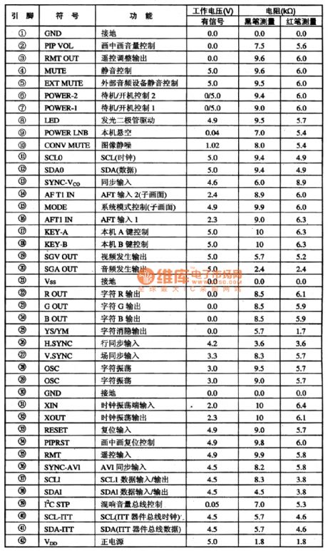
MC68HSO5P4DW-Communication single chip microcomputer integrated circuit diagram
Published:2011/5/22 1:58:00 Author:leo | Keyword: MC68HSO5P4DW-Communication single chip microcomputer integrated circuit diagram
MC68HSO5P4DW is a kind of communication single chip microcomputer integrated circuit produced by Motorola in USA which is widely applied in wireless telephones.
1.Function features:The integrated circuit MC68HSO5P4DW is used to carry out impulse, two-tone compatible dial, input and output of various control signals, receiving detection and manually/automatically converting of various command signals.
2.Pin function and data:The integrated circuit MC68HSO5P4DW adopts 28-pin duel lie patch package. The picture gives the detailed information about its pin function and related data. (View)
View full Circuit Diagram | Comments | Reading(564)
Application input end zeroing circuit diagram
Published:2011/5/17 1:43:00 Author:Rebekka | Keyword: Application input end , zeroing circuit
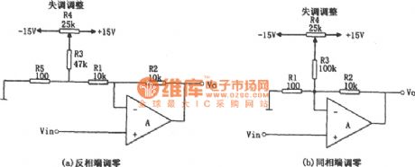
In figure (a), it uses a small resistor R5 connecting in the return circuit of R1, the offset voltage produced by R5 and R3 are added to the left end of R1.And the voltage will be divided by R1 and R2. So the offset voltage adjustment range is determined by the following formula: Offset voltage adjustment range = ± VD · (R5/R3) · (R2 / (Rl + R2)) (± VD = ± l5V).
According to the resistance value shown in figure (a) , the offset voltage adjustment range is: ± 15mV. R1 = R2. Therefore, the voltage gain of the circuit is low. Taking the R5 and R1 are in series into account , the voltage gain Av: Av = 1 + R2 / (Rl + R5) (View)
View full Circuit Diagram | Comments | Reading(641)
High-performance medium-level circuit composed of L1590 and CX2501
Published:2011/5/13 1:34:00 Author:Rebekka | Keyword: High-performance medium-level
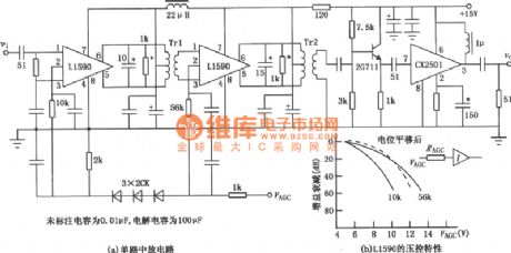
In the discharge circuit is high-performance. It is applicable to the medium-level which is particularly stringent required in making. It can also be used in medium-level of general receiver. The features of the circuit is: High gain, wide AGC range, high load capacity, high reliability and simple circuit. When the circuit is used in pairs, the amplitude frequency and phase frequency characteristics consistency of the two-way medium-level can achieve a very high target. (View)
View full Circuit Diagram | Comments | Reading(683)
Pulse delay circuit circuit diagram
Published:2011/5/12 6:23:00 Author:Rebekka | Keyword: Pulse delay circuit
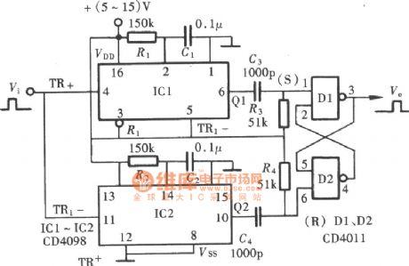
If you need to delay longer than the input pulse width of the pulse delay circuit, you can use pulse delay circuit composed of the NAND gate and single-shot. Its composition is shown in the figure. (View)
View full Circuit Diagram | Comments | Reading(2129)
Delay circuit with fixed-frequency coefficients
Published:2011/5/12 5:52:00 Author:Rebekka | Keyword: Delay circuit , fixed-frequency coefficients
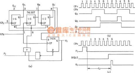
Figure is Delay circuit with fixed-frequency coefficients. The circuit is composed of the 60 divider and D flip-flop 7474. 74LS57 has a 10 frequency divider that composed of an independent 6 divider, a 5 frequency and a 2 frequency level. Its output ends are QA, QB and QC. (View)
View full Circuit Diagram | Comments | Reading(1821)
Precision addition circuit composed of INA105
Published:2011/5/11 22:22:00 Author:Rebekka | Keyword: Precision addition
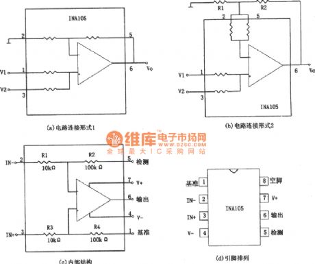
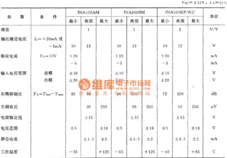
Precision addition circuit composed of INA105 is shown as above.
The main parameters of INA05 series is shown as above. (View)
View full Circuit Diagram | Comments | Reading(619)
Common adder circuit diagram
Published:2011/5/11 4:02:00 Author:Rebekka | Keyword: Common adder
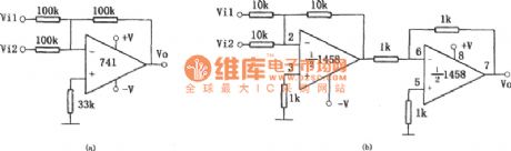
Common adder(741 1458) circuit diagram is shown as above.
Figure (a) is the inverting addition circuit, the input-output relationship is: Vo =- (Vil + Vi2).When you need the same addition, you can use the circuit shown in figure (b), the input-output relationship is: Vo = Vil + Vi2. (View)
View full Circuit Diagram | Comments | Reading(966)
Capacitors Measured with Composite Pipe Circuit
Published:2011/5/10 2:22:00 Author:Felicity | Keyword: Capacitors Measured with Composite Pipe Circuit,
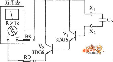
The picture above shows the Capacitors Measured with Composite Pipe Circuit . (View)
View full Circuit Diagram | Comments | Reading(547)
| Pages:10/13 12345678910111213 |
Circuit Categories
power supply circuit
Amplifier Circuit
Basic Circuit
LED and Light Circuit
Sensor Circuit
Signal Processing
Electrical Equipment Circuit
Control Circuit
Remote Control Circuit
A/D-D/A Converter Circuit
Audio Circuit
Measuring and Test Circuit
Communication Circuit
Computer-Related Circuit
555 Circuit
Automotive Circuit
Repairing Circuit