
Circuit Diagram
Index 1469
The thyristor voltage regulation circuit with the output power of 1-4KvA
Published:2011/7/20 22:15:00 Author:Borg | Keyword: voltage regulation circuit, output power
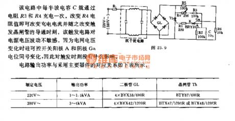
The capacitor C in the circuit is charged by R3 and R4 every half wave. The charge current changes if the resistance of R4 is changed, and the conducting time of the trigger thyristor is changed. The trigger circuit is not sensitive to the power supply voltage deviation. As the LEV of the positive pole A and negative pole Ga of the SCR switch changes when the grid voltage changes, so it doesn't affect the trigger time.
(View)
View full Circuit Diagram | Comments | Reading(711)
The data general line test circuit
Published:2011/7/20 22:07:00 Author:Borg | Keyword: general line
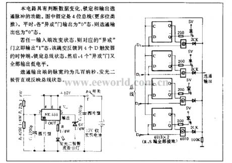
The circuit can judge the data change, lock and output the strobe pulse. In the figure, we assume it is the 4-bit general line(more bit analogy). Usually, each OR gate outputs 0 , and the strobe output is also 0 . If each input terminal changes its state, the corresponding OR gate will output 1 quickly, the jump is fed back to 4 clock terminals of D trigger, which locates the general line. Then, all of the 4 OR gates output the low LEV.
(View)
View full Circuit Diagram | Comments | Reading(667)
the digital separation circuit
Published:2011/7/20 21:58:00 Author:Borg | Keyword: digital separation circuit
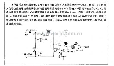
The circuit is fixed with a photoelectric coupler, which can fully separate the electricity between 2 digital circuits. The low voltage input signal of +4V can also change the output state, and the circuit can afford the peak value of +100V without being broken down. Q1 and Q2 compose the current stabilizer, which limits the current at 7mA through the input terminal of the photoelectric separator. The Zener diode CR2 provides with the Vref which decides the current of R2.
(View)
View full Circuit Diagram | Comments | Reading(624)
the digital clock circuit
Published:2011/7/20 21:51:00 Author:Borg | Keyword: digital clock
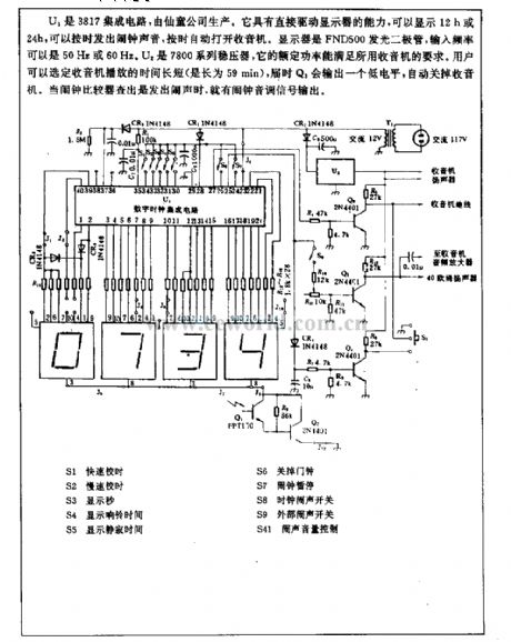
U1 is a 3817 integrated circuit, which is produced by Fairchild Corp. It can directly drive the display, and it can display for 12h or 24h, It can generate the clock sound and turn on the radios on time. The display is a FND500 LED, the input frequency can be 50Hz or 60hz. U2 is a 7800 voltage stabilizer whose regulated power can meet all radio users' need. The users can choose the radio working time length(the max time is 59min).
(View)
View full Circuit Diagram | Comments | Reading(2221)
Xinke 5300A Power Amplifier Front And Central Sound-Channel Silent Repairing Circuit
Published:2011/7/24 10:07:00 Author:Robert | Keyword: Xinke, 5300A, Power Amplifier, Sound-Channel, Silent, Repairing
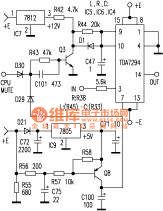
This device is a universal AV power amplifier certified by Dolby. The device's all kinds of functions and operation display is managed by a CPU (UPD78042). The selected audio signal would be send to NJW1103 for decoding after the buffer, and it would output L, R, C S four channel signals. The first two signals would be send separately to a single-chip integrated power amplifier TDA7294 for amplification after the Dolby/direct selection, balance, volume control, pre-amplification (LM833). However the central and the surround channel signals would be amplified and volume controlled directly by the LM833 and then are send to the end integrated power amplifier for amplification (C is TDA7294 and S is TDA7265). Also when starting the CPU's MUTE port will send the squelch signal and then do the squelch for each TDA7294 and TDA7265 through the squelch circuit. (View)
View full Circuit Diagram | Comments | Reading(1300)
the digital pulse width test circuit
Published:2011/7/20 21:44:00 Author:Borg | Keyword: pulse width, test circuit
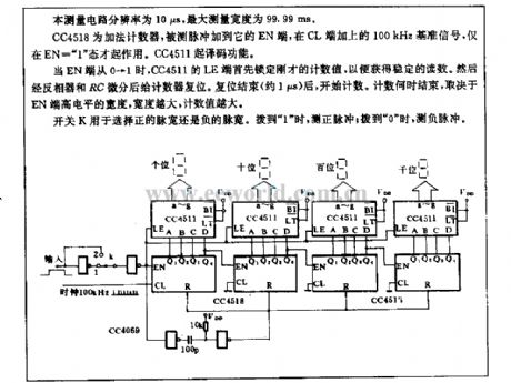
The definition of the test circuit is 10μs, the Max test width is 99.99ms. CC4518 is the adding counter, the pulsed under test is added on its EN terminal, the 100kHz reference signal is added on the CL terminal, only when EN=1 does the counter work. CC4511 works as the decoder. When EN changes from 0 to 1, the LE of CC4511 locates the counting number firstly, so the stable reading can be acquired. Then the counter is reset after it is differentiated by the phase reverser and RC.
(View)
View full Circuit Diagram | Comments | Reading(672)
the digital watch circuit
Published:2011/7/20 21:34:00 Author:Borg | Keyword: digital watch
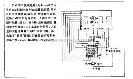
The ICM7200 integrated circuit (produced by Intersil Corp.) connects with the screen in multi-channel method, the user can selectively display the H, M, S or the date. This CMOS chip contains a long binary counter, which splits the 32.768KHz crystal oscillator input signal into the 1s reference clock signal. The other counters generate the H, M and date. When the key of see the time is pressed for the first time, the watch will display the hour and minute; when it is pressed for the second time, the watch will display the date and the second will be displayed for the third time.
(View)
View full Circuit Diagram | Comments | Reading(1705)
Operational Amplifier Basic Circuit
Published:2011/7/26 7:27:00 Author:Robert | Keyword: Operational, Amplifier, Basic
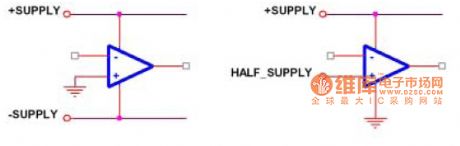
The positive power pin is connected to VCC+ and the ground or VCC- pin is connected to the GND. By taking a half of the positive voltage as virtual ground to connect to the operational amplifier's input pin, then the output voltage would be this virtual ground's voltage. And the operational amplifier's output voltage would take the virtual ground as center between the swing of Vom. There are some new operational amplifiers having two different maximum output voltage and minimum output voltage. This operational amplifier's data sheet would specifically point the Voh and Vol separately. It should be noted that many designers would use the virtual ground arbitrarily as reference for the input voltage and output voltage. But in most applications, the input and output use the power supply ground as reference. So the designers must add a DC-isolated capacitor in the input part and output part to isolate the DC voltage between the virtual ground and ground. (View)
View full Circuit Diagram | Comments | Reading(718)
The pilotless car circuit of double motors
Published:2011/7/20 21:24:00 Author:Borg | Keyword: pilotless car
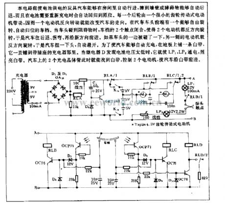
The circuit can make the toy car with battery power supply move automatically, and the toy car can back off automatically when it touches the wall or the obstacle, it will reset automatically when the cell needs to be recharged. Each rear wheel is driven by a wheel gear motor, so just the reversed running of one motor can control the moving direction of the car. At the head of the car, there is a car gear which can freely rotate and reset automatically.
(View)
View full Circuit Diagram | Comments | Reading(689)
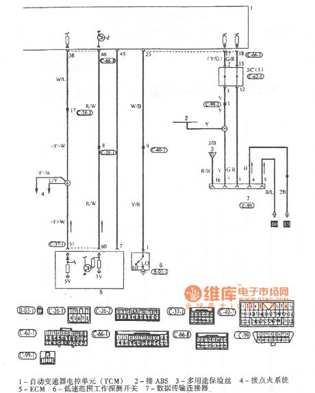
Buick GL8 Car ABS Stopping Lamp Switch Input And Torque Circuit
Published:2011/7/24 10:09:00 Author:Robert | Keyword: Buick, GL8, Car, ABS, Stopping Lamp, Switch, Input, Torque
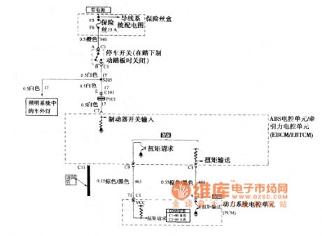
The picture shows the Buick GL8 car ABS stopping lamp switch input and torque circuit. (View)
View full Circuit Diagram | Comments | Reading(472)
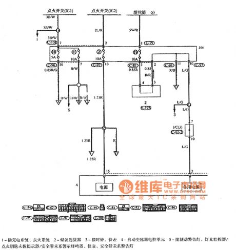
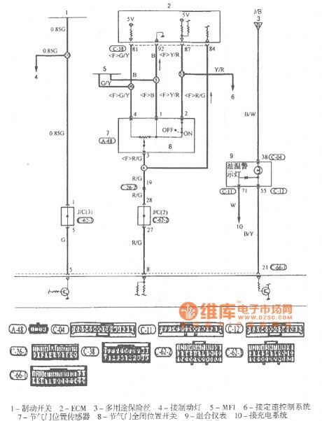
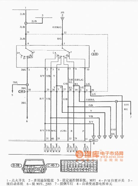
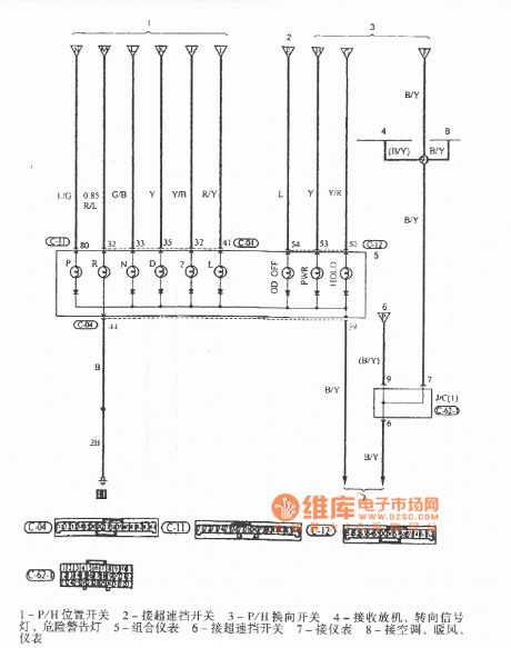
Cheetah SUV Automatic Transmission Circuit
Published:2011/7/26 8:08:00 Author:Robert | Keyword: Cheetah, SUV, Automatic, Transmission
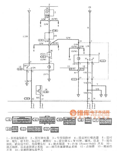
The pictures show the Cheetah SUV automatic transmission circuits.
In picture 1 the part 1 is connected to the charging system and ignition system. The part 2 is reserve connector. The part 3 is connected to clock and instruments. The part 4 is automatic transmission ECU. The part 5 is connected to brake alarm lamp, the light monitor, ignition key not-pulling reminder, seat belt not-tying alarm buzzer, instrument, seat belt not-tying alarm lamp.
In picture 2 the part 1 is brake switch. The part 2 is ECM. The part 3 is multi-purpose fuse. The part 4 is connected to the brake lamp. The part 5 is MFI. The part 6 is connected to constant speed control system. The part 7 is throttle position sensor. The part 8 is throttle full-closing position switch. The part 9 is instrument cluster. The part 10 is connected to charging system.
In picture 3 the part 1 is multi-purpose fuse. The part 2 is rear lamp relay. The part 3 is special fuse. The part 4 is connected to front lamp washers. The part 5 is connected to clock, rear lamp, parking lamp, logo lamp, license plate lamp. The part 6 is connected to air conditioner. The part 7 is connected to radio, turning signal lamp, danger alarm lamp. And so on. (View)
View full Circuit Diagram | Comments | Reading(606)
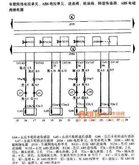
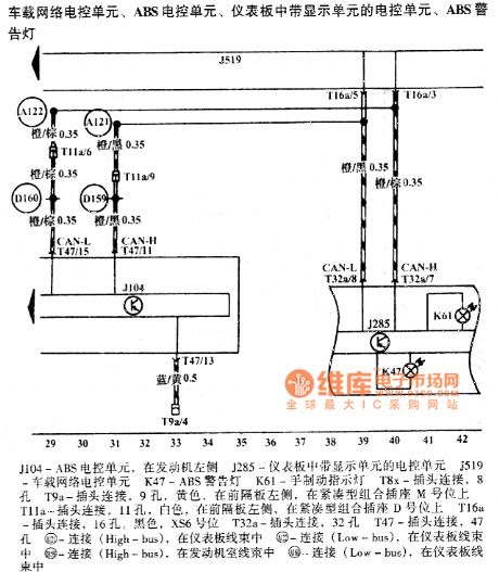
Polo ABS Circuit
Published:2011/7/26 8:26:00 Author:Robert | Keyword: Polo, ABS
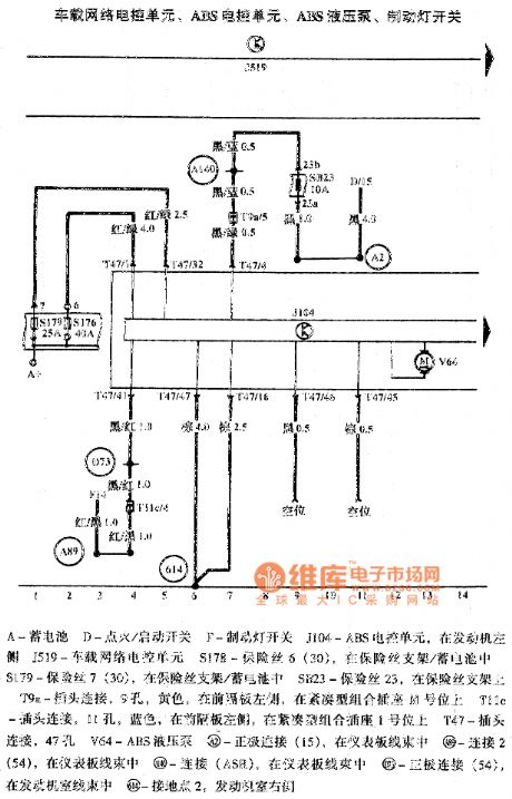
The pictures show the Polo ABS circuit.
The first picture shows the car network ECU, ABS ECU, ABS hydraulic pump, brake lamp switch.
The second picture shows the car network ECU, ABS ECU, oil-feed pump, oil drain pump, rotationl speed sensor, ABS electromagnetic pump relay.
The third picture shows the car network ECU, ABS ECU, dashboard ECU with display unit, ABS alarm lamp. In the picture the J104 is ABS ECU which is at the left side of engine. The J285 is dashboard ECU with display unit. The J519 is car network ECU. The K47 is ABS alarm lamp. The K61 is hand brake lamp. And so on. (View)
View full Circuit Diagram | Comments | Reading(1950)
The solar auto tracking control circuit
Published:2011/7/20 20:40:00 Author:Borg | Keyword: solar, auto tracking, control circuit
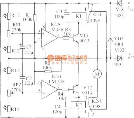
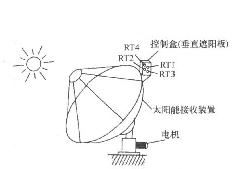
See as the figure, the dual op-amp LM358 composes 2 voltage comparator with R1 and R2, the Vref is 1/2 of VDD(+12V). The LDR of RT1 and RT2 with RP1, RT3 and RT4 with RP2 compose the light dependent sensing circuit respectively, one special thing of the circuit is that it can automatically self-compensate according to the light. See as the figure, RT1 and RT3 are installed at one side of longitudinal sunshading board, while RT4 and RT2 at the other side.
(View)
View full Circuit Diagram | Comments | Reading(3654)
The general counter circuit
Published:2011/7/20 21:11:00 Author:Borg | Keyword: general counter
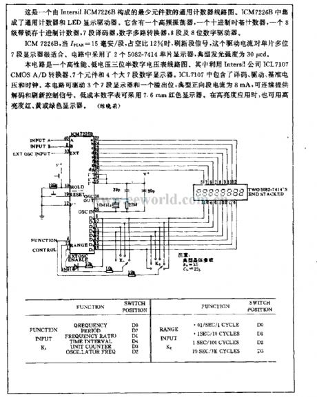
This is a general counter circuit with the least elements, which consists of Intersil ICM7226B. ICM7226B integrates the general counter and the LED display driver, it contains a HF oscillator, a decimal time-based counter, an octal lock decimal counter, 7-stage decoder, digital multi-channel converter, 8-stage and 8-bit digit driver. When Ipeak=15mA/S, duty cycle is 12%, ICM7226B will refresh the stage signal.
(View)
View full Circuit Diagram | Comments | Reading(715)
The auto control energy saving lamp circuit composed of solar battery
Published:2011/7/20 20:48:00 Author:Borg | Keyword: energy saving lamp, solar battery
See as the figure, the solar auto control energy saving lamp circuit consists of the solar cell charger, light control switch, timing switch and reversing circuit. To light the energy-saveing lamp, both the light control and timing switches are connected. At daytime, the sunlight is shed on the solar cell board, which converts the light power into electricity and charges the storage cell with the help of the diode VD1. (View)
View full Circuit Diagram | Comments | Reading(1640)
Temperature controller 6
Published:2011/7/25 21:45:00 Author:Ecco | Keyword: Temperature controller
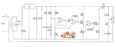
The temperature controller circuit is composed of the power supply circuit, temperature detection control circuit and control implementation circuit, and it is shown as the chart. Power supply circuit is composed of the power switch S, power transformer T, bridge rectifier UR, filter capacitors Cl ~ C3, three-terminal voltage regulator integrated circuit IC1, resistor R2 and power indicator LED YL1. Temperature detection control circuit is composed of the temperature detection diode VD1, resistors R3 ~ R1O, operational amplifier integrated circuit IC2 (N1 ~ N3) and the potentiometer RP. Control implementation circuit is composed of the resistors R11, R12, transistor V and thyristor VT.
(View)
View full Circuit Diagram | Comments | Reading(596)
Temperature controller 7
Published:2011/7/25 21:49:00 Author:Ecco | Keyword: Temperature controller
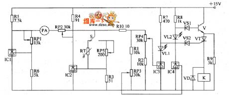
The temperature controller circuit is composed of the temperature detection circuit and temperature control circuit, and it is shown as the chart. Temperature detection circuit is composed of the temperature sensor (thermistor) RT, three-terminal precision regulators ICl, IC2, potentiometers RP1, RP2, RP5, ammeter (temperature indication with) PA, resistors R3 ~ R5 and temperature measurement / set switch. Temperature control circuit consists of three-terminal precision regulators IC3, IC4, transistor V, thyristor VT, voltage regulator diodes VS1, VS2, relay K, diode VD, LEDs VL1, VL2, resistors RI, R2, R7 ~ RIO and temperature UCL potentiometers RP3, RP4, temperature LC potentiometer.
(View)
View full Circuit Diagram | Comments | Reading(604)
Temperature controller 8
Published:2011/7/25 21:51:00 Author:Ecco | Keyword: Temperature controller
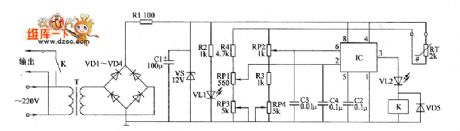
The temperature controller circuit is composed of the power supply circuit and temperature detection control circuit, and it is shown as the chart. Power supply circuit is composed of the power transformer T, rectifier diodes VD1 ~ VD4, resistors RI, power indicator LED VL1, filter capacitor C1 and Zener VS and so on. Temperature detection control circuit consists of thermistor RT, time-base integrated circuit IC, potentiometers RP1 ~ RP4, resistors R2 ~ R4, capacitors C2 ~ CZ, relay Kl, diode VD5 and light emitting diode VL2.
(View)
View full Circuit Diagram | Comments | Reading(653)
Temperature controller 9
Published:2011/7/25 21:54:00 Author:Ecco | Keyword: Temperature controller
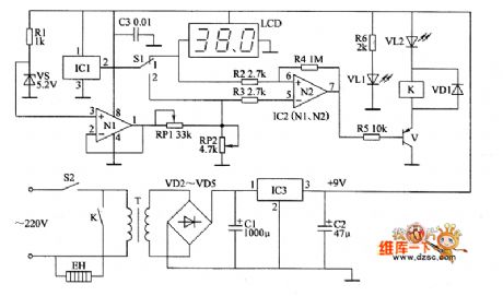
The temperature controller circuit is composed of the power supply circuit, temperature detection / display circuit, reference voltage circuit and control circuit, and it is shown as the chart. Power supply circuit is composed of the power switch S2, power transformer T, rectifier diodes VD2 ~ VD5, filter capacitors C1, C2, three-terminal voltage regulator integrated circuit IC3, resistors R6 and power indicator LED VL1. Temperature detection / display circuit is composed of the temperature sensor integrated circuit IC1, the control switch S1 and LCD display.
(View)
View full Circuit Diagram | Comments | Reading(694)
Timing controller circuit diagram 3
Published:2011/7/26 2:04:00 Author:Ecco | Keyword: Timing controller

The timing controller circuit is composed of the power supply circuit and timing control circuit, and it is shown as the chart. Power supply circuit is composed of the power control button S1, normally open contact K1 of relay K, buck capacitor C1, discharge resistor R1, rectifier diodes VD1 ~ VD4, filter capacitor C2 and zener diode VS. Timing control circuit is composed of the time-base integrated circuit IC, delaying time selection switch S2, resistors R2 ~ R5, capacitors C3, C4, light-emitting diode VL, relay K and diode VD5.
(View)
View full Circuit Diagram | Comments | Reading(733)
| Pages:1469/2234 At 2014611462146314641465146614671468146914701471147214731474147514761477147814791480Under 20 |
Circuit Categories
power supply circuit
Amplifier Circuit
Basic Circuit
LED and Light Circuit
Sensor Circuit
Signal Processing
Electrical Equipment Circuit
Control Circuit
Remote Control Circuit
A/D-D/A Converter Circuit
Audio Circuit
Measuring and Test Circuit
Communication Circuit
Computer-Related Circuit
555 Circuit
Automotive Circuit
Repairing Circuit