
Circuit Diagram
Index 1472
Electrical Pulse Therapeutic Apparatus (the 4th)
Published:2011/7/16 0:38:00 Author:Felicity | Keyword: Electrical Pulse, Therapeutic Apparatus
Work of the circuit
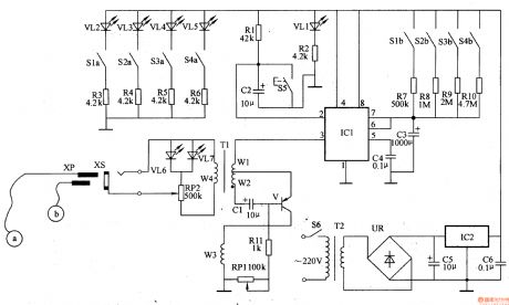
The circuit consists of power supply circuit, timing circuit and pulse voltage generator circuit. (It is showed in the picture 9-4.)
Power supply circuit consists of power switch S6, power transformer T2, bridge rectifier, UR, resistors Rl, filter capacitors C5 and C6, power indicator LED VLl and three-terminal regulator IC lC2.
Timing circuit consists of resistors Rl, R3-RlO, LED VL2-VL5, capacitors C2-C4, timer switch Sl-S4, when the reset button 55 and the base integrated circuit IC1.
Pulse voltage generator circuit consists of Transistor V, resistors Rll, potentiometer RPl, RP2, capacitor Cl, pulse transformer Tl, work instructions LED VL6, VL7, socket XS, XP, and the plug electrode a, b. (View)
View full Circuit Diagram | Comments | Reading(617)
Heart Rhythm Tester (the 2nd)
Published:2011/7/17 5:04:00 Author:Felicity | Keyword: Heart Rhythm Tester, the 2nd
Work of the circuit
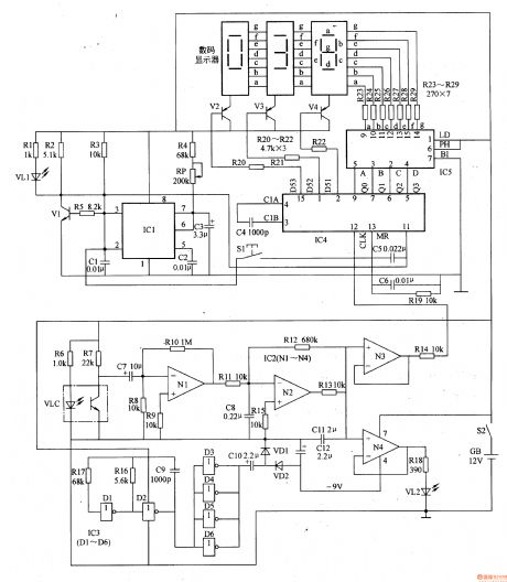
The circuit consists of infrared testing amplifying circuit, negative voltage producing circuit, working indicating circuit, timing circuit and digit displaying driving circuit. (It is showed in picture 9-54.)
Infrared testing amplifying circuit consists of infrared optocoupler (infrared sensor) VLC, resistors R6-Rl5, capacitors C7, C8, and Nl-N3 within the operational amplifier integrated circuit lC2 (Nl-N4).
Negative voltage producing circuit consists of six non-gate integrated circuit IC3 (Dl-D6), resistors Rl6, R17, capacitor Cg-C11 and diode VDl, VD2.
Working indicating circuit consists of capacitor Cll, IC2 internal op amp N4, resistors R18 and power indicator LED VL2.
Timing circuit consists of time-base integrated circuit rCl, resistors R1-R5, potentiometer RP, capacitors Cl-C3, light-emitting diodes VLl and transistors Vl.
Digit displaying driving circuit consists of digital displays, transistors V2-V4, resistors R2O-R29, capacitors C4-C6, counter display driver integrated circuit IC4and decoding circuit IC5.
Turn on power switch S2 and the battery GB will provide +l2V working voltage to ICl-IC5. Oscillating signal is shaped and rectified. It then provides -9V voltage to IC2.
When you do the test put your finger on the reflexing window of VLC. Infrared signal goes through the soft tissue and reflexes on phalanx. The infrared photosensitive transistor receives the signal and turns it into electronic signals. The digital displayer starts working and N4 drives VL2 flash. After the regular time (30s) is over, the counter stops working. Double of the figure on the displayer is the tester’s heart rhythm. (View)
View full Circuit Diagram | Comments | Reading(995)
Heart Rhythm Tester (the 1st)
Published:2011/7/17 5:29:00 Author:Felicity | Keyword: Heart Rhythm Tester

Heart Rhythm Tester (the 1st)
Work of the circuit
The circuit consists of blood flow runoff testing amplifying circuit, datum voltage circuit, comparing amplifying circuit, stable circuit, LED indicating circuit and power circuit. (It is shows in picture 9-53.)
Blood flow runoff testing amplifying circuit consists of resistor R3-R9, capacitor C2-C6, light-emitting diodes VLl, photosensitive resistor RG and Nl, N2 within the operational amplifier integrated circuit IC1 (Nl-N4).
Datum voltage circuit consists of resistors Rl, R2, R9, RlO, capacitor C7, IC1's internal operational amplifier N4and potentiometer RP.
Stable circuit consists of time-base integrated circuit IC2, diode VD2, capacitor C9, ClO, and resistors R13, R14.
LED indicating circuit consists of resistor Rl5, R16, transistors V and light emitting diodes VU.
When you do the test, put your finger on the testing sensor. The sensor consists of VL1 and RG. RG tests the signal voltage of the blood runoff. The signal is transited to N3 through N1 and N2. It produces positive impulse and negative impulse. It makes V work intermittently. It makes VL2 shines. The shining rate is the heart rhythm.
Change the value of RP to change the sensitivity of the circuit.
(View)
View full Circuit Diagram | Comments | Reading(604)
Pulse Test Set (the 3rd)
Published:2011/7/17 5:33:00 Author:Felicity | Keyword: Pulse Test Set
Work of the circuit
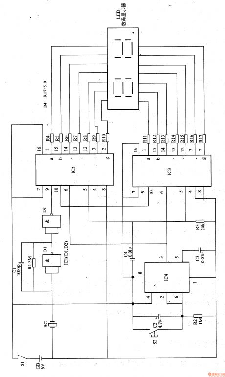
The circuit consists of pulse signal dealing circuit, timing circuit and display driving circuit. (It is showed in picture 9-50.)
Pulse signal dealing circuit consists of piezoelectric ceramics BC (as sensors), resistors Rl, capacitor Cl and NAND gate integrated circuit ICl (Dl, D2).
Timing circuit consists of reset button S2, capacitors C2-C4, resistor R2 and time-base integrated circuit IC4.
Display driving circuit consists of display driver integrated circuit IC2, 1C3, resistors R3-R17 and digital display.
When you turn on the power switch S1, IC2 and IC3 are minimum clearing. Put BC on the position where the pulse is significant. BC changes the pulse signal to electronic signal. Press S2 and C2 discharges quickly through S2. IC2 and IC3 start counting. The number which is displayed on the LED digital display is the jumping number of times of pulse per minute. (View)
View full Circuit Diagram | Comments | Reading(567)
Electric Medical Attracting Controlling Circuit (the 1st)
Published:2011/7/16 0:33:00 Author:Felicity | Keyword: Electric Medical, Attracting Controlling Circuit
Work of the circuit
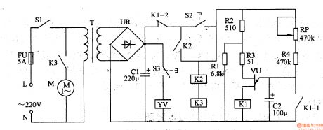
The circuit consists of power circuit and controlling circuit. (It is showed in picture 9-43.)
Press button S2. K2 and K3 are electrified. Vacuum pump motor M starts to work. At the same time the +24V voltage on C1 supplies power to C2 through Kl-2、S2、RP and R4. When the voltage on C2 reaches the largest voltage of VU, M stops working. And KL-1 of K1 is turned on. C2 discharges through KL-1 quickly and is prepared for next time of working.
When the negative pressure bottle gets the negative pressure, the user could press S3 to control the use of negative pressure. If the negative pressure is not enough for use, the use can press S2 again. (View)
View full Circuit Diagram | Comments | Reading(561)
Dangerous Area Warning Device (the 2nd)
Published:2011/7/17 1:04:00 Author:Felicity | Keyword: Dangerous Area Warning Device
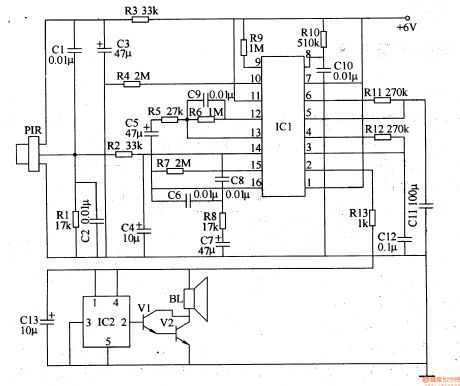
Work of the circuit
The circuit consists of pyroelectric infrared sensor (PIR), the signal processing circuit and the language reminding circuit.(It is showed in the picture 8-122.)
The signal processing circuit consists of pyroelectric infrared signal processing integrated circuit ICI , resistor M-Rl2 and capacitors C4-Cl2.
The language reminding circuit consists of voice IC IC2, transistors Vl and V2, resistor R13, capacitor C13 and the speaker BL.
When no one is in the warning area, the no signal is inputted at pin 14 of IC1. Its pin 2 is of low level. The language reminding circuit does not work. (View)
View full Circuit Diagram | Comments | Reading(658)
High-voltage Electrostatic Generator (the 2nd)
Published:2011/7/16 0:40:00 Author:Felicity | Keyword: High-voltage Electrostatic, Generator
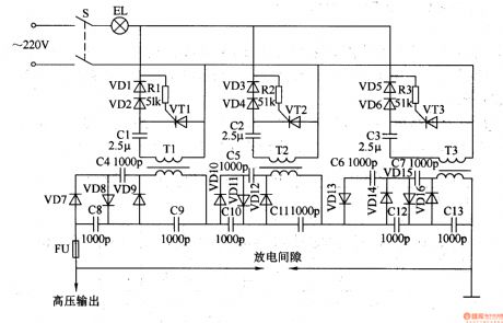
Work of the circuit
The circuit consists of oscillation step-up circuit and voltage doubler rectifier circuit. (It is showed in the picture 8-116.)
Oscillation step-up circuit consists of Resistors Rl-R3, capacitor Cl-C3, thyristor VTl-VT3, diode VDl-VD6 and step-up transformer Tl-T3.
Voltage doubler rectifier circuit consists of diode VD7-VDl6 and capacitors C4-Cl3.
When the high-voltage generator is working, sparks are produced in the discharge gap (gap is adjustable). This can limit the outputting voltage. It can also indicate whether the outputting voltage is zero or not. (View)
View full Circuit Diagram | Comments | Reading(2603)
Automotive Fuel Monitor Five
Published:2011/7/17 5:56:00 Author:Felicity | Keyword: Automotive Fuel Monitor
The circuit consists of oil level monitoring circuit, the oil level indicating circuit and lacking fuel alarm circuit.
Oil level monitoring circuit consists of automotive fuel tank float potentiometer RP, resistors Rl, R2 and capacitor C.
The oil level indicating circuit consists of R3-R8, RlO-R13, LED VL1-VL4 and quad op amp IC IC (Nl-N4).
Lacking fuel alarm circuit consists of resistor R9, transistor V and buzzer HA.
The voltage divider circuit consist of R3-R8 and the circuit provides standard oil level voltage for the non-inverting terminal of N1-N4 inside IC; The voltage divided by R1 and RP and then put on to inverting terminal of N1-N4 through R2 as the oil amount sample voltage.
When the fuel tank is full of oil, the resistance of RP is at its lowest and N1, N3, N4 output high level voltage, VL2 output low level voltage. And the yellow LED VL2 is on indicating the fuel tank is full.
When the tank is 3/4 full, N3 also output low level voltage to make green led VL3 on.
When the tank is 1/2 full, N4 also output low level voltage to make green led VL4 on.
When the tank is 1/4 full, N1 also output low level voltage to make red led VL1 and V on. And the beeper beeps to remind the driver to refuel. (View)
View full Circuit Diagram | Comments | Reading(864)
Automotive Fuel Monitor Two
Published:2011/7/17 6:04:00 Author:Felicity | Keyword: Automotive Fuel Monitor
The circuit consists of comparator, the monostable flip-flop and warning lamp circuit. (It is showed in picture 7-59.)
Comparator consists of divider circuit (by the resistors Rl-R3 form) and integrated operational amplifier circuit ICl.
The monostable flip-flop consists of time-base integrated circuit IC2 and the peripheral components.
Warning lamp circuit consists of transistor Vl, V2, and light-emitting diode VL.
Pin 2 (inverting terminal) of IC1 is connected to the center head of RP,the potentiometer, through R4.
When the fuel is enough, pin 6 of IC 1is at high level ,V1 and V2 both cut off.
When the amount of fuel is below a certain value, pin 6 is at low level. And then V1 and V2 is on to light up LED VL; The monostable flip-flop inside IC2 flip, changing from steady-state into transient-state. Pin 3 of IC3 is at high level,and the beeper HA works.
When C3 is end of charge, IC is at steady-state again. Pin 3 is at low level and HA stops. But LED VL shines until the fule tank is refilled. (View)
View full Circuit Diagram | Comments | Reading(583)
Trigger Circuit of Devices
Published:2011/7/16 0:41:00 Author:Felicity | Keyword: Trigger
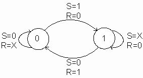
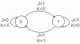
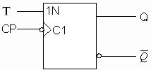
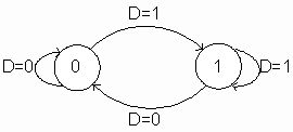
We have three ways to describe the logical function of trigger. First is characteristic equation. Second is characteristic table and the third one is state transition diagram. (showed in picture 1,2,3,4)
Picture 1 shows the state transition diagram of RS Trigger.
Picture2 shows the state transition diagram ofJK Trigger.
Picture3 shows the state transition diagram and logical symbol ofJK Trigger.
Picture4 shows the state transition diagram ofD Trigger.
Characteristics table is actually a special kind of truth table and it has a very specific description of trigger.The input variables (independent variables)of truth table are not only data entry but also initial states of flip-flop. And the output variable (dependent variable) is the next state flip-flop. Characteristic equation is out from the feature table summarizes so it's more concise. State transition diagramwhich describes the methodsis very intuitive. (View)
View full Circuit Diagram | Comments | Reading(812)
Ward Caller Eight
Published:2011/7/17 0:46:00 Author:Felicity | Keyword: Ward Caller
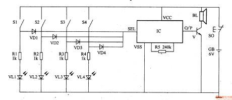
This ward caller is consists of calling-control circuit and music circuit.
Aalling-control circuit consists of callswitchesSl-S4,resistorsR1-R4,light-emitting diodesVLl-VL4anddiodeVDl-VD4.
Music circuit consists of resistorR5,transistorV,musicintegrated circuitIC andspeaker BL .
When one of the call switches S1-S4 is pressed, the IC is triggered on to work, the music electrical signal output by O/P is amplified by V to drive BL to send out music
sound; at the same time the LED in this branch is on to indicate the bed number of the patient. After the medical personnel receives the acousto-optic calling signal, they
reset S2 and press the reset button S0 to make IC reset and BL stops.
Only four calling circuitsare showed in the figure and the number of it can be adjusted according to actual need. (View)
View full Circuit Diagram | Comments | Reading(576)
Ward Caller Six
Published:2011/7/17 0:53:00 Author:Felicity | Keyword: Ward Caller
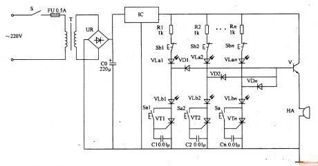
Work of the circuit
The circuit consists of power circuit, call control circuit and light and sound call circuit. (It is showed in picture 9-89.)
Power circuit consists of Power switch S, fuse FU, power transformer T, bridge rectifier, UR, filter capacitor CO and three-terminal regulator IC IC.
Call control circuit consists of control buttons Sa1-San, capacitors Cl-Cn, thyristor VTl-VT2 and light-emitting diode VLal, VLan.
Light and sound call circuit consists of resistors Rl-Rn, reset button Sbl-Sbn, LED VLbl-VLbn, diode VDl-VDn, transistor V and buzzer HA.
When Sal-San are not pressed, VT1-VTn and V are all cut off and VLa1-VLan and VLa1-VLbn are off, and HA is noiseless.
When one of Sa1-San is pressed, the thyristor connect to it is triggered on and the LED in this branch is on to indicate the patient bed number. At the same time V is
saturated and on. HA beeps. While the medical personnel receives the ward calling signal , they press the reset button, and the thyristor and the transistor cut off, and the
two LEDs are off, then HA stop beeping.
(View)
View full Circuit Diagram | Comments | Reading(590)
Patient SOS Appliance One
Published:2011/7/17 1:00:00 Author:Felicity | Keyword: Patient SOS Appliance
Work of the circuit
The circuit consists of SOS trigger circuit, sound and light alarm circuit and audio amplifier output circuit. (It is showed in picture 9-82.)
SOS trigger circuit consists of SOS switch S2, the trigger switch S3, the transistor Vl-V3, and the peripheral components.
Sound and light alarm circuit consists of audio integrated circuits ICl, resistors R6 and light-emitting diode VLl, VL2.
Audio amplifier output circuit consists of boost the audio power amplifier module IC2, super loudness piezoelectric buzzer HA, resistor R7 and diode VD2.
When the user is in the normal state, the power switch and calling switch is on, and the trigger switch S3 is off. V1 is saturated and on and V2 and V3 cut off. IC2 and IC3 are both off, and the beeper HA is noiseless. LED VL1 and VL2 are off. When the user is ill and fall down, S3 is on, and V1 cut off. V2 and V3 are on. IC1 and IC2 is power on and at work. The beeper HA sends out the whistle sound of ambulance and at the same time LED VL1 and VL2 are on and light the words ‘HELP’ and ‘Medicine is in the box’ on the first aid panel up. (View)
View full Circuit Diagram | Comments | Reading(1036)
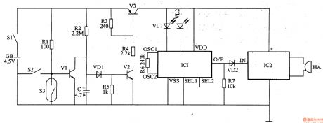
Eye-care Lamps (the 6th)
Published:2011/7/17 4:37:00 Author:Felicity | Keyword: Eye-care Lamps
Work of the circuit
The circuit consists of power circuit, infrared radiation circuit, infrared reception and amplifying circuit, rectifying circuit, electric switch circuit , function control circuit and so on (It is showed in picture 9-73.).
Power circuit consists of power transformer T, bridge rectifier, UR, filter capacitors C3, C4, C5, current limiting resistor R6, R7 and Zener VS.
Infrared radiation circuit consists of resistors R3-R5, capacitor C2, transistor V2, V3 and infrared light-emitting diode VLl.
Infrared reception amplifying circuit consists of infrared photodiode VDl, resistors Rg-Rll, capacitors C6, C7 and transistor V4, V5.
Rectifying circuit consists of capacitor C9, ClO, resistors R13, R14 and diode VD2, VD3.
Electric switch circuit consists of resistor R2, R8, capacitor Cll, transistor V6, V7 and thyristor Vm.
Sound alarm circuit consists of resistors R5, R6, capacitors C2-known, the transistor V8, Vg and speaker BL.
Function control circuit consists of Function switch SL resistors Rl, potentiometers RPl, capacitor Cl, two-way trigger diode VlO and thyristor VTl.
When the user’s read-write distance is ok, the voice alarm circuit doesn’t work. When the user’s read-write distance is too near BL will alarm.
When the environmental light is good VL2 does not work. But if the environmental light is poor for reading and writing VL will be lighten to remind the user. (View)
View full Circuit Diagram | Comments | Reading(540)
Car Windshield Wiper Controller (the 4th)
Published:2011/7/17 4:41:00 Author:Felicity | Keyword: Car Windshield Wiper Controller
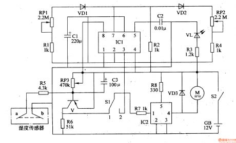
Work of the circuit
The circuit consists of humidity examining circuit, electric switch control circuit and Multivibrator (It is showed in the picture 7-166.).
Humidity examining circuit consists of humidity sensors, transistors v, resistors R5, R6, potentiometer RP3and capacitor C3.
Electric switch control circuit consists of electronic switch integrated circuit IC2, function switch Sl, resistors R7, R8 and diode VD3.
Multivibrator consists of time-base integrated circuit ICl, resistors Rl, R2, R4, potentiometer RPl, RP2, capacitor Cl, C2 and diode VDl, VD2.
When the switch is off the motor is out of work. When it is rainy the electric switch within IC2 is turned on and M starts to work. When the rain is over the electric switch within IC2 is turned off. And M stops working. S2 is the power switch so you should turn it off when the car is not moving. (View)
View full Circuit Diagram | Comments | Reading(641)
Wiring circuit diagram of operational amplifier application circuit input
Published:2011/7/16 9:44:00 Author:Sophia | Keyword: Operational amplifier application circuit input, Wiring
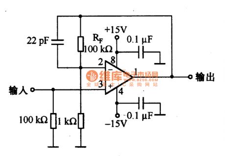
The wiring of op-amp applications circuit inputsThe impedance of Op amp's inverting input and the non-inverting inputare high, the input wiring should be short, otherwise, the external electrostatic and electromagnetic induction will generate noise. Figure is the in-phase amplifier circuit with phase gain of 40dB; the impedance of inverting input is high, if the wiring of this part is too long, which will lead to noise.So feedback resistor RF and Rs should be connected close to the inverting input to make the part of the high-impedance bea short connection. (View)
View full Circuit Diagram | Comments | Reading(936)
Drunken Driving Limiter (the 3rd)
Published:2011/7/17 4:49:00 Author:Felicity | Keyword: Drunken Driving Limiter, the 3rd
Work of the circuit
The circuit consists of power circuit, alcoholic testing circuit, sound circuit, sound amplifying and outputting circuit and igniting circuit. (It is showed in picture 7-162.)
Power circuit consists of battery GB, diode VDl, resistors Rl, power indicator LED VLl, filter capacitor Cl, C2, and three-terminal regulator integrator ICl.
Alcoholic testing circuit consists of wine-sensitive sensor, potentiometer and the electronic switch circuit IC2 RP.
Sound circuit consists of resistors R3-R5 and voice integrated circuits lC3.
Sound amplifying and outputting circuit consists of capacitor C3-C5, audio power amplifier integrated circuit IC4, speaker BL, LED Vl2 and VL3 and resistor R2.
Igniting circuit consists of capacitors C6 and relay K.
If the driver is drunk and wants to turn on S. IC1 tests the sense of alcohol. The electric resistance will become smaller. The electronic switch within IC1 is turned on. IC3 and IC4 starts to work. IC3 outputs the sound signal which is amplified by IC4. The signal drives BL make the sound that “Please do not drive when you are drunk.” VL2 and VL3 start shining. The power circuit of igniting circuit is cut off. The driver cannot start the car. (View)
View full Circuit Diagram | Comments | Reading(636)
Impedance matching circuit diagram of high-frequency circuit test
Published:2011/7/16 9:38:00 Author:Sophia | Keyword: High-frequency circuit test, Impedance matching
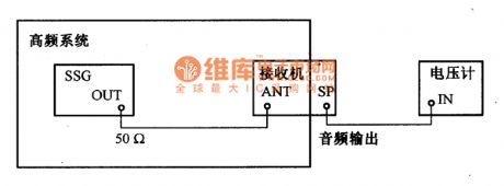
When High-frequency circuit is tested, its impedance match of cable, testers are very important.Impedance usually is 5OΩ or 75Ω. The diagram is the basic connection type to measure the receiver sensitivity. The impedance of the receiver usually is 50Ω, so the output impedance of standard signal generator(SSG) also should be 5OΩ. We should notice the following points: the connecting impedance of the measuring equipment should be identical; the impedance of electric cable should be identical; connector should have excellent impedance chracteristic within the limits of measuring frequency; the cable should be as short as possible; high-powered tester should be adopted; the output terminal of SSG should connect high-frequency fuse wire. (View)
View full Circuit Diagram | Comments | Reading(628)
Frequency characteristic of shunt capacitance circuit diagram
Published:2011/7/16 9:39:00 Author:Sophia | Keyword: Shunt capacitance, Frequency characteristic

Power supply decoupling circuit usually adopts shunt capacitance and choose the optimum capacity and variety according to the frequency band of the circuits. Especially in high frequency circuit, shunt capacitance can reduce the power supply impedance, so the choice of the capacitor should choose deliberately. The diagram is the impedance and frequency chacateristic of ceramic capacitor. Theoretically, the capacitor impedance is 1/(2πfC). But the higher capacitance, the higher frequency, the lower impedance. because of the influence of the internal impedance, in excess of regular frequency, the impedance of the real capacitor will be higher on the contrary. So when the impedance reach the lowest point, the capacitance will be low and the frequency will be the highest. In the diagram a and b, when the capacitance is 10000pF, the frequency is 10MHZ; when the capacitance is 1000pF, the frequency is 40MHZ. When the frequency is high, shunt capacitance adopts low capacity capacitance, which will have better effect than high capacity.
(View)
View full Circuit Diagram | Comments | Reading(692)
Single-supply operation of the operational amplifier input protection circuit
Published:2011/7/16 9:41:00 Author:Sophia | Keyword: Single-supply operation, the operational amplifier input protection
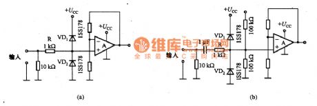
The diagram a, b is a single-supply op amp input protection circuit, the diode VD2 is connected between the op amp input and the ground. In Figure (a) and Figure (b) the resistance R is 1kΩ, but in low-noise circuit, which the circuit performance is influenced by the thermal noise of the resistance itself, the smaller the resistance R of 100Ω resistance, the smaller the effect of Thermal noise. (View)
View full Circuit Diagram | Comments | Reading(1595)
| Pages:1472/2234 At 2014611462146314641465146614671468146914701471147214731474147514761477147814791480Under 20 |
Circuit Categories
power supply circuit
Amplifier Circuit
Basic Circuit
LED and Light Circuit
Sensor Circuit
Signal Processing
Electrical Equipment Circuit
Control Circuit
Remote Control Circuit
A/D-D/A Converter Circuit
Audio Circuit
Measuring and Test Circuit
Communication Circuit
Computer-Related Circuit
555 Circuit
Automotive Circuit
Repairing Circuit