
Circuit Diagram
Index 832
LOW_FREQUENCY_PRESCALER
Published:2009/7/10 3:10:00 Author:May
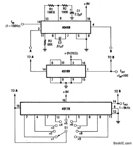
For multiplying frequencies in the 1-to 150-Hz range, this circuit uses a 4046B and a + 100 prescaler. The VCO output is phaselocked to the low-frequency input. This simplifies use of a frequency counter to measure LF signal frequencies.
By using a 4017B and a 1-kHz fIN, the circuit can be used as a 1-to 9-kHz frequency synthesizer or as a x 10 frequency multiplier. (View)
View full Circuit Diagram | Comments | Reading(1051)
PROJECTILE_ACCELERATION_TELEMETER
Published:2009/7/19 22:27:00 Author:Jessie
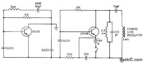
Microwave signal at 24,000 Mc is aimed down barrel of howitzer by sheet aluminum reflector that is replaced abet each firing. Variations in reflection coefficient of ferrite device on projectile nose modulate reflected micro-wave signal from moving projectile, at frequency dependent on acceleration. Circuit shows encapsulated transducer mounted on nose. Capacitance gage produces frequency shift of 70-kc subcarrier that is proportional to acceleration, for driving ferrite-core modulator through amplifier stage.-W. M. Kendrick and L. A. Peters, Projectile Telemetry with Microwaves, Electronics, 33;38, p 68-71.
(View)
View full Circuit Diagram | Comments | Reading(1091)
ANALOG_TACHOMETER_READOUT
Published:2009/7/10 3:10:00 Author:May
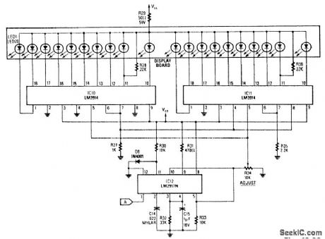
The analog display consists of a frequency/voltage converter (IC12) and bar-graph segment drivers IC10 and IC11. R34 is the calibration adjustment and is set so that an engine rpm of 5000 to 7000 rpm lights the first LED (redline value). (View)
View full Circuit Diagram | Comments | Reading(3134)
μA2240_STAIRCASE_GENERATOR
Published:2009/7/10 3:08:00 Author:May

The μA2240 timer/counter, combined with a precision resistor ladder network and an op amp, form the staircase generator. In the astable mode, once a trigger pulse is applied, the μA2240 operates continuously until it receives a reset pulse. The trigger input at pin 11 is tied to the time base output at pin 14, resulting in automatic starting and continuous operation. The frequency of the time-base oscillator, TBO, is set by the time constants R1 and C1 ( f=1/R1C1). For this example, a 10-KΩ) resistor and a 0.01-μF capacitor form the timing network.The counter outputs are connected to a precision resistor ladder network with binary-weighted resistors. The current sink through the resistors connected to the counter outputs correspond to the count number. For example, the current sink at Q7, the most significant bit, is 128 times the current sink at Q0, the least significant bit. As the count is generated by the μA2240 eight-bit counter, the current sink through each active binary-weighted resistor decreases the positive output of the op amp in discrete steps.The feedback potentiometer is set at a nominal 10 KΩ to supply a maximum output voltage range. An input of 12 V allows a 10-V output swing. With a 0.5-V input reference on pin 3 of the TCL271, the output will change front 10.46 V maximum, in 256 steps of 38.9 mV per step, to a 0.5 V minimum. Each step has a pulse duration of 100 μs and an amplitude decrease of 38.9 mV. The waveform output is repeated until a reset is applied to the μA2240. (View)
View full Circuit Diagram | Comments | Reading(1349)
_10V_TO__05V
Published:2009/7/19 22:26:00 Author:Jessie
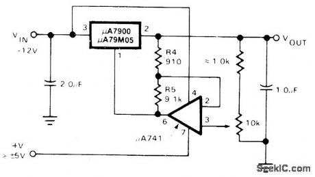
Regulator in μA7900 series is used with 741 opamp to provide adjustable output voltage. Differential between input and output is 2V.- Signetics Analog Data Manual, SignetIcs, Sunnyvale, CA, 1977, p 670. (View)
View full Circuit Diagram | Comments | Reading(578)
2_KC_COLD_CATHODE_COUNT_RATE_CIRCUIT
Published:2009/7/19 22:26:00 Author:Jessie
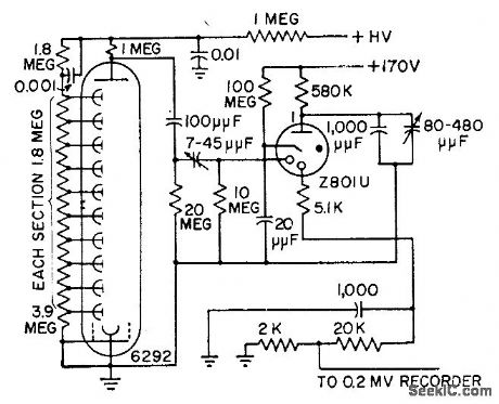
Uses triode having separate cold-cathode diode that produces glow discharge to eliminate trigger-cathode gap of triode section. This eliminates photosensitivity shown by most cold-cathode devices. Maximum operating speed is 2,000 counts per second.-M. H.Goosey, Designing Cold-Cathode Tube Circuits, Electronics, 31:3, p 101-108. (View)
View full Circuit Diagram | Comments | Reading(716)
SOUND_ACTIVATED_SWITCH
Published:2009/7/10 3:08:00 Author:May
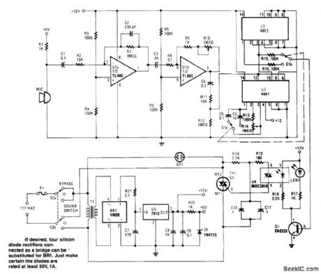
This circuit provides either latched switching or timed switching.U1A and U1B provide audio ampliftcation from the microphone,U2 is a retriggerable monostable multivibrator. S1A and S1B select either U3,a flip-flop,or U2. R13 and R14 allow a 6- to 60-second timer delay after the sound ceases,in the timed mode。BR1,U5,and associated components form a power supply.Q1 drives optocoupler U4 andtriggers triac TR1. (View)
View full Circuit Diagram | Comments | Reading(0)
POST_DETECTION_DIVERSITY_COMBINER
Published:2009/7/19 22:25:00 Author:Jessie
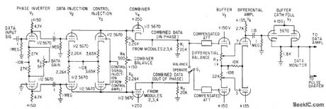
Can handle any IRIG modulating signal and feed any telemetry receiver having external agc output. Will combine two, three, or four channels.-W. Casson and R. C. Robinson, Versatile Diversity Combiner Handles Most Missile-Range Signals, Electronics, 35:44, p 40-43.
(View)
View full Circuit Diagram | Comments | Reading(1315)
PREFERRED_ASTABLE_BLOCKING_OSCILLATOR
Published:2009/7/19 22:25:00 Author:Jessie
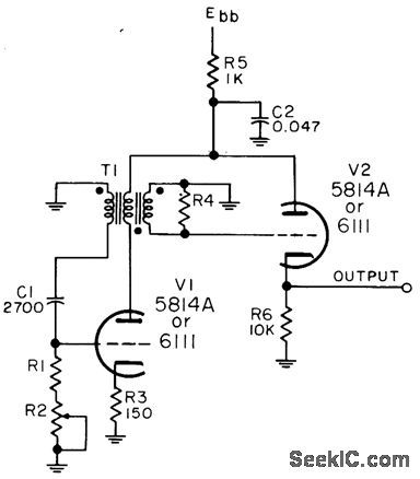
Used as pulse generator when frequency stability is not important. Output can be used as trigger without further shaping. R4 should be maximum that will just suppress ringing. Design equations are given for R1 and R2, but final values must be determined experimentally. Range is 200 to 2,000 pps. Output is positive.-NBS, Handbook Preferred Circuits Navy Aeronautical Electronic Equipment, Vol, I, Electron Tube Circuits, 1963, PC 48, p 48-2. (View)
View full Circuit Diagram | Comments | Reading(1005)
DATA_ACQUISITION_SYSTEM_Ⅱ
Published:2009/7/10 3:08:00 Author:May
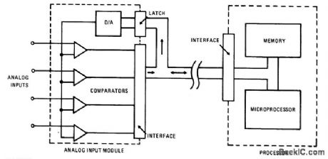
In this circuit, an HA-4900 series comparator is used in conjunction with a D/A converter to form a simple, versatile, multichannel analog input for a data acquisition system. The processor first sends an address to the D/A, then the processor reads the digital word generated by the comparator outputs. lb perform a simple comparison, the processor sets the D/A to a given reference level, then examines one or more comparator outputs to determine if the inputs are above or below the reference. A window comparison consists of two such cycles with two reference levels set by the D/A. 0ne way to digitize the inputs would be for the processor to increment the D/A in steps. The DiA address, as each comparator switches, is the digitized level of the input. While stairstepping, the D/A is slower than successive approximation; all chan-nels are digitized during one staircase ramp. (View)
View full Circuit Diagram | Comments | Reading(611)
CODE_PRACTICE_OSCILLATOR_Ⅲ
Published:2009/7/10 3:07:00 Author:May
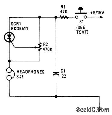
Capacitor C1 charges through resistor R1, and when the gate level established by potentiometer R2 is high enough, the SCR is triggered. Current flows through the SCR and earphones, discharging C1. The anode voltage and current drop to a low level, so the SCR stops conducting and the cycle is repeated. Resistor R2 lets the gate potential across C1 be adjusted, which charges the frequency or tone, Use a pair of 8-Ω headphones. The telegraph key goes right into the B+ line, 9-V battery. (View)
View full Circuit Diagram | Comments | Reading(632)
5_24V
Published:2009/7/19 22:25:00 Author:Jessie
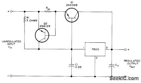
Choice of regulator in 7800 series determines value of output voltage that is maintained within 0.05% of its actual value. Choose regulator for voltage desired. Unregulated input Vin must be at least 2 V higher than regulator rating. Transient suppression capacitor CT is typically 10 to 50 μF. Output current is increased above IC rating by using PNP series-pass transistor Q1 which has maximum collector current of 30 A. Protection circuit Q2 pre-vents burnout of power transistor. Choose RSC for limiting current value to desired value.-J.E. Trulove, Three-Terminal Voltage-Regulator ICs, Ham Radio, Dec. 1973, p 26-30. (View)
View full Circuit Diagram | Comments | Reading(929)
MICRO_MULTIPLEXER
Published:2009/7/19 22:24:00 Author:Jessie
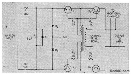
Solid-state high speed time-division commutator connects several low-level inputs, one at a time, to common differential bus. Each multiplexor channel consists of two transistor switch pairs.-J. V. Dirocco und J. W. Peghiny, Low-Level Encoding Approach: Latest Details of Titan II Telemetry, Electron'Ics, 35:47, p 36-39. (View)
View full Circuit Diagram | Comments | Reading(895)
DATA_ACQUISITION_SYSTEM_I
Published:2009/7/10 3:07:00 Author:May
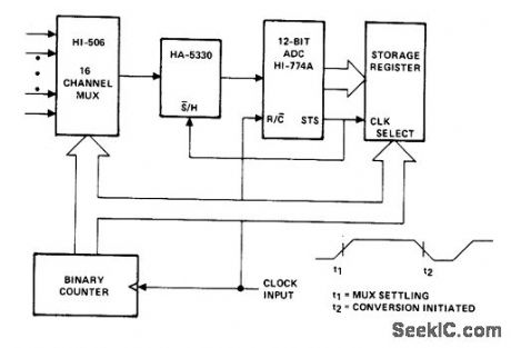
The Hl-506 multiplexer is used as an analog input selector, controlled by a binary counter to address the appropriate channel. The HA-5330 is a high-speed sample and hold. The sample/hold control is tied to the status (STS) output of the HI-774A; whenever a conversion is in process, the S/H is in the hold mode. A conversion is initiated when the clock input becomes low; when the clock becomes high, the mux address changes. The mux will be acquiring the next channel while the ADO is converting the present input, held by the SiH. The clock low time should be between 225 ns and 6.5 ps, with the period greater than 8.5 μs.
With this timing, T/C will be high at the end of a conversion, so the output data will be valid ~ 100 ns before STS goes low. This allows STS to clock the data into the storage register. The register address will be offset by one; if this is a problem, a 4-bit latch can be added to the input of the storage register. With a 100-kHz clock rate, each channel will be read every 160 μs. (View)
View full Circuit Diagram | Comments | Reading(720)
8_to_170_KC_WITH_PLUG_IN_CRYSTALS
Published:2009/7/19 22:23:00 Author:Jessie
Oscillator frequency can be changed by replacing crystal and one capacitor in feedback loop. Stability is obtained from squaring transistor Q1 which feeds crystal.-R. Couvela, Oscillator Frequency is Changed by Plug-In Units, Electronics, 34:36, p 86-87. (View)
View full Circuit Diagram | Comments | Reading(716)
CAPACITOR_ESR_MEASURER
Published:2009/7/10 3:07:00 Author:May
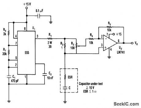
The equivalent series resistance (ESR) of a capacitor can be measured using this circuit and an ac voltmeter. U1 functions as a 50-kHz square-wave generator. It drives a current waveform of about ±180mA in the capacitor-under-test, through R1 and R2. When R3 is adjusted to the proper value, the voltage drop across the equivalent series resistor is precisely nulled by the inverting amplifier (U2). Thus, VO is the pure capacitor voltage which is the minimum voltage that can be produced at VO.
To make an ac voltage measurement, adjust R3 until VO is minimized. Then, note the position of the potentiometer and multiply it by the value of R2, 1Ω in this case. That product equals the capacitor's ESR. The capacitor is biased at about 7.5 V. Lower-voltage capacitors won't work with this circuit. By changing the value of R2, other ranges of ESR can be measured. However, for small R2 values, the current level should be increased to keep a reasonable voltage across R2. This requires some sort of buffer. The circuit is intended for capacitors greater than 100μF. The ripple voltage gets large for smaller values and accuracy decreases. (View)
View full Circuit Diagram | Comments | Reading(1222)
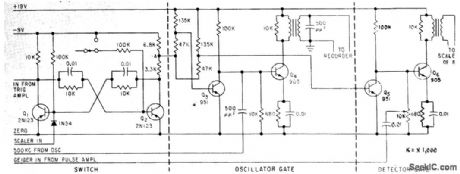
BASIC_SCALER
Published:2009/7/19 22:23:00 Author:Jessie
Each staler stage is bistable circuit with trigger amplifiers between each pair of stages. Used to make 512 counts from ion chamber give one output to telemetry system.-D. Enemark, Balloon-Borne Circuits Sort High-Altiiude Cosmic Rays, Electronics, 32:35, p 52-55. (View)
View full Circuit Diagram | Comments | Reading(1291)
3_WIRE_RECEIVER_MESSAGE_DEMUXER
Published:2009/7/10 3:05:00 Author:May
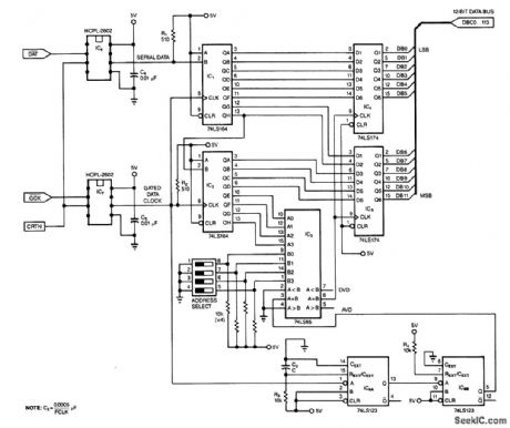
This 3-wire receiver checks the first four data bits of 16 received bits against a preset address. If the two match, the remaining 12 bits are latched into two 6-bit flip-flop registers. Either CMOS or TTL logic families can be used in the design. (View)
View full Circuit Diagram | Comments | Reading(668)
RADIOACTIVE_FUEL_FLOW_GAGE
Published:2009/7/19 22:23:00 Author:Jessie
Used in recording flow rate of let fuel containing radioactive tracer.-J. D. Keys and G. E. Alexander, Radioactive Tracers Find Jet Fuel Flow Roles, Electronics, 33:8, 58-59. (View)
View full Circuit Diagram | Comments | Reading(635)
AUDIO_OSCLLATOR
Published:2009/7/10 3:03:00 Author:May
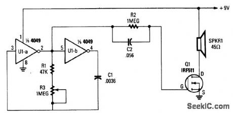
Two gates, U1A and U1B (1/3 of a 4049 hex inveter), are connected in a VFO circuit. Components R1, R3, and C1 set the frequency range of the VFO. With the values given, the circuit's output can range from a few hundred hertz to over several thousand hertz by adjusting R3.
The simplest way to change the frequency range of the oscillator is to use different capacitance values for C1. A rotary switch, teamed up with a number of capacitors, can be used to select the desired fre-quency range. (View)
View full Circuit Diagram | Comments | Reading(926)
| Pages:832/2234 At 20821822823824825826827828829830831832833834835836837838839840Under 20 |
Circuit Categories
power supply circuit
Amplifier Circuit
Basic Circuit
LED and Light Circuit
Sensor Circuit
Signal Processing
Electrical Equipment Circuit
Control Circuit
Remote Control Circuit
A/D-D/A Converter Circuit
Audio Circuit
Measuring and Test Circuit
Communication Circuit
Computer-Related Circuit
555 Circuit
Automotive Circuit
Repairing Circuit