
Index 202
The basic application circuit of MAX690A/692A
Published:2011/6/28 21:13:00 Author:qqtang | Keyword: application circuit
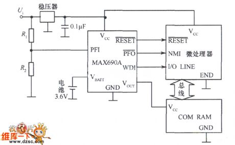
View full Circuit Diagram | Comments | Reading(942)
W7663/7664 regulator series, main features and pin of DC-DC circuit and power supply monitor
Published:2011/6/27 5:32:00 Author:Lucas | Keyword: regulator series, main features , pin, DC-DC circuit , power supply, monitor
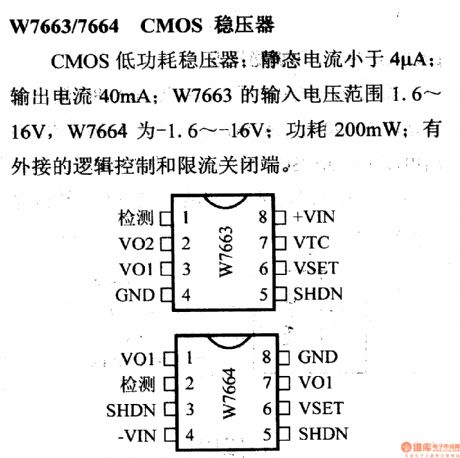
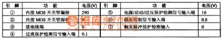
W7663/7664 CMOS regulators.
CMOS low-power voltage regulator; quiescent current is less than 4μA; output current is 40mA; W7663 input voltage range is 1.6 ~ 16V, W7664 is -1. 6 ~-16V; power consumption is 200mW; it has external logic control and current limiting closing sides.
(View)
View full Circuit Diagram | Comments | Reading(633)
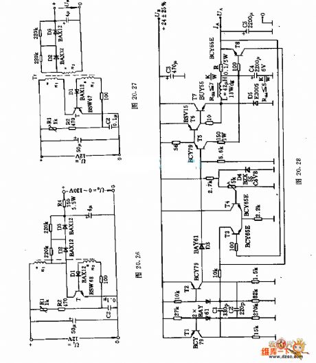
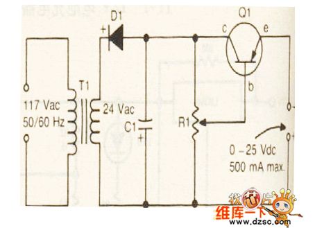
The 6v-12v/25w DC voltage converter circuit (1)
Published:2011/6/28 21:58:00 Author:qqtang | Keyword: 6v-12v/25w, DC voltage converter
(View)
View full Circuit Diagram | Comments | Reading(754)
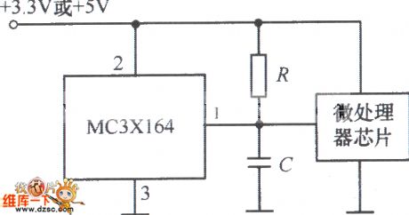
The reset circuit of MC3X164
Published:2011/6/28 21:59:00 Author:qqtang | Keyword: reset circuit
View full Circuit Diagram | Comments | Reading(674)
The circuit of the specialized voltage monitor integrated chip MAX791
Published:2011/6/28 22:15:00 Author:qqtang | Keyword: specialized, voltage monitor, integrated chip
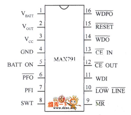
View full Circuit Diagram | Comments | Reading(698)
The 1.5V precise regulated power supply circuit
Published:2011/6/28 22:21:00 Author:qqtang | Keyword: precise, regulated power supply
View full Circuit Diagram | Comments | Reading(788)
Two ends delay switch circuit with the LM122
Published:2011/6/19 19:40:00 Author:TaoXi | Keyword: Two ends, delay, switch
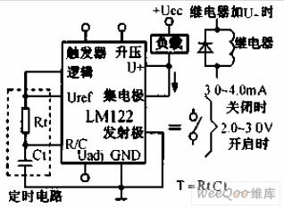
The two ends delay switch circuit with the LM122 is as shown in the figure, the LM122 integrated timer can be used as the two ends delay switch component. When the LM122 integrated timer is in the conduction state, the voltage drop is 2 to 3V, the current can be 50mA. The circuit function is: if you add the power supply voltage and after the delay time of R1C1 seconds, the relay conducts. The disconnecting current of the timer is about 3 to 4mA.
(View)
View full Circuit Diagram | Comments | Reading(572)
Integrated regulated power supply circuit diagram
Published:2011/6/27 5:00:00 Author:Ecco | Keyword: Integrated , regulated , power supply
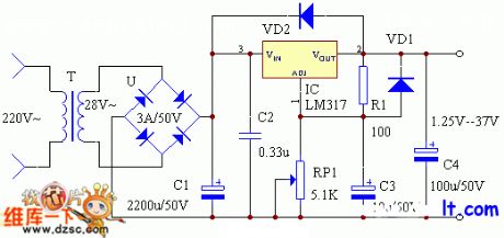
This is a continuously adjustable output voltage integrated power supply, and the output voltage is continuously adjustable between 1.25-37V, and the maximum output current is up to 1.5A. Circuit is simple and suitable for self-made by electronic lovers. It can be used for a variety of small electrical power supply. LM317 output current is 1.5A, the output voltage can be adjusted continuously between 1.25-37V, and the output voltage is set by two external resistors R1, RP1, and the voltage difference between the output end and adjusting end is 1.25V, and the voltage will produce a few milliamps of current.
(View)
View full Circuit Diagram | Comments | Reading(738)
High-efficiency 70W universal switching power supply module circuit diagram
Published:2011/6/27 4:03:00 Author:Ecco | Keyword: High-efficiency , 70W , universal , switching power supply , module
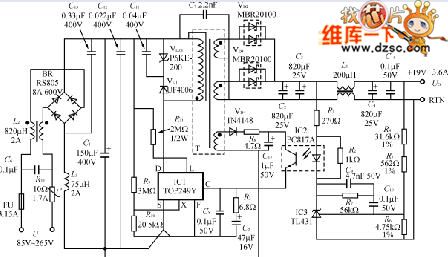
TOPSwitch GX is suitable for making low-cost, high efficiency, small size, full-enclosed switching power supply module or power adapter (adapter). When the ambient temperature does not exceed 40 ℃, the module can be reduced to the dimensions of 10.5mm × 5.5mm × 2.5mm. The AC input voltage range is 85V ~ 265V, which is a common worldwide voltage range. Rated output power is PO = 70W; load regulation is SI = ± 4%; power efficiency is η ≥ 84% (when the AC input voltage U = 85V, full load efficiency is 85%; when U = 230V, the power efficiency is up to 90% ); load power consumption is <0.52W (U = 230V pm).
(View)
View full Circuit Diagram | Comments | Reading(6512)
45 W multi-output switching power supply circuit diagram composed of TOP246Y
Published:2011/6/27 3:59:00 Author:Ecco | Keyword: 45 W , multi-output , switching, power supply
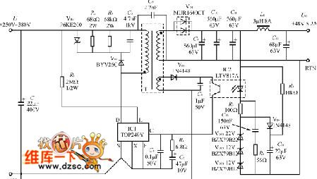
It can be used as set-top box, cable decoder, high-capacity hard disk drive or laptop computer switching power supply. The power supply input voltage is AC 185V ~ 265V, and the rated output power is 45W, and the peak output power is up to 60W; power efficiency is η ≥ 75%, no-load power consumption is only 0.6W. Five outputs are: UO1 (5V, 3.2A), UO2 (3.3V, 3A), UO3 (30V, 0.03A), UO4 (18V, 0.5A), UO5 (12V, 0.6A); their load regulation rates are ± 5%, ± 5%, ± 8%, ± 7%, ± 7%.
(View)
View full Circuit Diagram | Comments | Reading(4955)
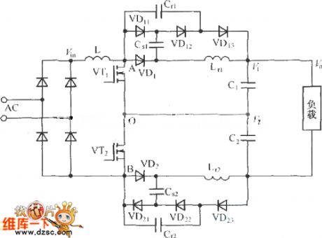
Three-level passive lossless soft-switch PFC topology circuit
Published:2011/6/27 19:38:00 Author:John | Keyword: soft-switch
View full Circuit Diagram | Comments | Reading(1265)
PFC lossless snubber main circuit
Published:2011/6/25 10:58:00 Author:John | Keyword: snubber
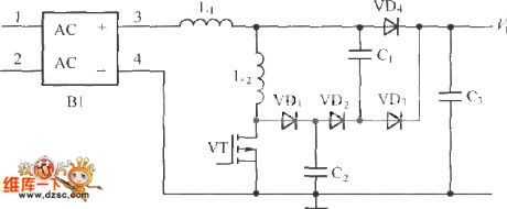
The charging process with normal charge mode is generally carried out in the home and public places. The normal charging mode’s charging power level is typically 6.6kW and its typical recharging time is 5 to 8 hours. The power converter of the normal charging mode is similar to that of the emergency charging mode. Normal charging mode also can use a single-stage AC / DC converter. However, with the single-stage PFC converter, the peak current of the switching tube is large. In the two converters, PFC Boost level can use to traditional Boost lifting circuit. The switch can be soft switch or hard switch.
(View)
View full Circuit Diagram | Comments | Reading(1799)
Simple Ni-MH battery charger circuit
Published:2011/6/21 0:12:00 Author:John | Keyword: Ni-MH battery charger
Simple Ni-MH battery charger circuit is shown.
(View)
View full Circuit Diagram | Comments | Reading(2701)
MODEM power supply circuit
Published:2011/6/19 2:49:00 Author:John | Keyword: power supply
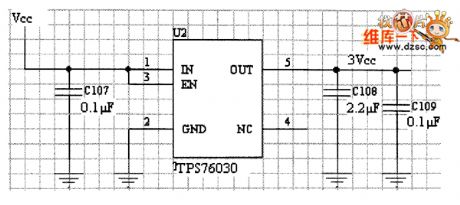
Despite of MODEM, the system is powered by 3.0V power supply. Such takes the power requirements on the hardware system with small ripple and stable voltage regulating functions into accounts. It also considers the low power consumption of hardware system. So the power part of the hardware system uses TI's TPS76330 chip, whose output current is 150mA. The system can meet current requirements. Besides, the chip has a small footprint, which can effectively save PCB board’s space. Power supply circuit is as shown in the figure.
To make the output power ripple be small, a 2.2μF and 0.1μF capacitors are set in the output section. Moreover, the other input end of the chip is also placed with a 0.1μF filter capacitor, thus reducing the disruption for the input end.
(View)
View full Circuit Diagram | Comments | Reading(644)
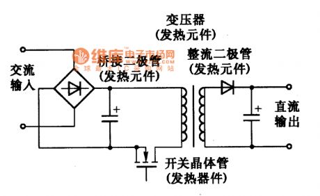
STR-M6833BFO4 switch power supply thick film integrated circuit
Published:2011/6/15 7:29:00 Author:chopper | Keyword: switch power supply, thick film, integrated circuit
STRM6833BFO4 is a switch power supply thick film integrated circuit produced (View)
View full Circuit Diagram | Comments | Reading(709)
groundwire style circuit
Published:2011/6/12 7:07:00 Author:chopper | Keyword: groundwire
Additionally,line filter which is used to control noise is connected to printed plate at the mains. And then,grounded common mode capacitor is fixed to the soleplate by screw.Lines are short and thick even if the current is not very big. On the printed plate are the lines of sunrise-style,just as the picture.Additionally,when the circuit adopts dual platen,it must switch in washer to guarantee the favorable contact.
(View)
View full Circuit Diagram | Comments | Reading(753)
STR-M6831AFO4 switch power supply thick film integrated circuit
Published:2011/6/15 7:41:00 Author:chopper | Keyword: switch power supply, thick film, integrated circuit

STRM6831AFO4 is a switch power supply thick film integrated circuit produced (View)
View full Circuit Diagram | Comments | Reading(903)
the line of printed plate should be wide enough when process big current circuit
Published:2011/6/12 7:19:00 Author:chopper | Keyword: line, printed plate, wide, big current
The line of printed plate should be wide enough when we deal with the big current.Generally speaking,line width of 1A current should be 1mm.And we can calculate by this rate.When the current is over 10A,we can calculate by the rate 0.7A/mm.As for the bold line of the following picture,there are biggish impact current through capacitor at the moment the power supply is connected even if the current is not big.Thus,the line should be wide enough.
(View)
View full Circuit Diagram | Comments | Reading(722)
STR-M6545LF switching power supply thick film integrated circuit
Published:2011/6/15 7:31:00 Author:chopper | Keyword: switching power supply, thick film
STRM6545LF is a mixed type switching power supply thick film integrated circu (View)
View full Circuit Diagram | Comments | Reading(656)
input voltage of three-terminal integrated regulator measure circuit
Published:2011/6/15 5:44:00 Author:chopper | Keyword: input voltage, three-terminal, integrated regulator, measure
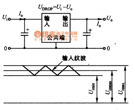
The following picture is a regulator circuit,the difference of input voltage and output voltage totally adds to the collector and emitter of controlled transistor.The output current is also the collector current of transistor.The power consumption of transistor Pc=I0 (Ui-U0),that is to say,the higher input voltage Vi is,the great power consumption of transistor is.The input voltage Uimin has to satisfy Uimin≥U0+UDROP.In the formula,UDROP is a voltage drop of the emitter and collector of transistor.Its lowest value is over the saturation voltage UCESAT of transistor.The UDROP of general regulator is about 30V,and regulator with low dropout is below 1V.
(View)
View full Circuit Diagram | Comments | Reading(769)
| Pages:202/291 At 20201202203204205206207208209210211212213214215216217218219220Under 20 |
Circuit Categories
power supply circuit
Amplifier Circuit
Basic Circuit
LED and Light Circuit
Sensor Circuit
Signal Processing
Electrical Equipment Circuit
Control Circuit
Remote Control Circuit
A/D-D/A Converter Circuit
Audio Circuit
Measuring and Test Circuit
Communication Circuit
Computer-Related Circuit
555 Circuit
Automotive Circuit
Repairing Circuit