
Index 215
Ni-Cd battery charge circuit consist of CD4040
Published:2011/6/1 5:16:00 Author:Crystal Liu | Keyword: Ni-Cd battery charge circuit , CD4040
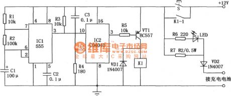
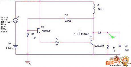
CD4040 counter chipformed the cadmium nickel battery charger as show in the picture. It can chargefor four quarter of cadmium nickel battery whoes capacity is 500mA , charge current charging time for 50mA, for l. five hours, and after finishing with charging the function of power. 555 time-based circuit constitute a clock signal generator, produce the l0Hz square wave signal, and its period for 6 seconds. When switching power supply, due to the 3 IC2 feet, so that the output low level VT1 semiconductor tube conduction, and make relay Kl suck close work, contact K1-1 closed, switch S in captive. Now charging current direction battery, and began to the battery. Status indicator LED lighted, said charging is ongoing.
CD4040 countermakes upfrequency divider and charging circuit. In the meanwhile, ICl switch on the power of the clock signal loss to produce the IC2 ⑩ feet, IC2 start counting. Because IC2 8192 was taken into the points: 1, therefore, only the frequency of an 8192 in counting pulse reach a IC2 feet by the (3) will only low level into high level, make VTl Kl stop work deadlines, and release the contacts K1-1, make it become disconnected from the state, bringing to a halt the charge. VD2 is used to prevent battery into circuit current reversed. (View)
View full Circuit Diagram | Comments | Reading(3249)
Current Amplifier Circuit Diagram made up of LF356 and Others
Published:2011/6/14 19:24:00 Author:leo | Keyword: Current Amplifier Circuit Diagram, LF356
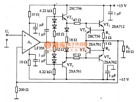
What the picture 1 shows is a current amplifier circuit made up of LF356 and so on. In the circuit, A1 is the backing amplifier while VT1 and VT2 (VT3 and VT4) can made up of the dual push-pull emitter follower circuit which amplifies DC signals with the frequency of 30 KHz and its output power is 1W. Vt5 and VT6 is used to protect power transistor when output circuit shorts. R1 is the sample and when the emitting polar current of VT3 and VT4 is 0.6A with the VT5 and VT6 on, VT5 and VT6 force the VT3 or VT4 to lower the base electric potential to protect the power transistor VT3 or VT4. (View)
View full Circuit Diagram | Comments | Reading(3633)
Constant Current Supply Circuit with Operational Amplifier
Published:2011/5/18 9:42:00 Author:Joyce | Keyword: Constant Current , Supply , with Operational Amplifier
View full Circuit Diagram | Comments | Reading(621)
simple and practical Boost circuit diagram
Published:2011/5/11 1:47:00 Author: | Keyword: simple, practical, Boost
View full Circuit Diagram | Comments | Reading(755)
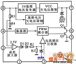
Multifunction Charger Four
Published:2011/5/19 8:08:00 Author:Michel | Keyword: Multifunction Charger Four
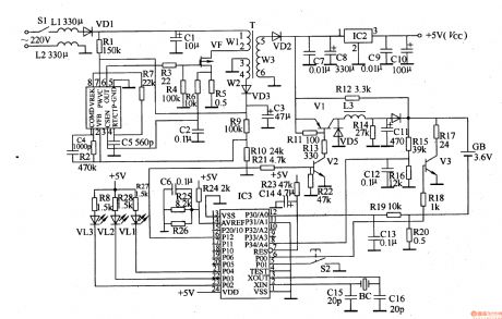
The multifunction charger introduced in the example takes advantage of switching power circuit and microprocessor (singlechip)control circuit with overcurrent and overvoltage protection functions.It can charge nickel-hydrogen and Lithium-ion rechargeable batteries.Circuit's Work PrincipleThis charger is composed of mains switch,S1,switching power circuit,control circuit,charge circuit and discharge circuit and it is showed as the picture 5-66.The switching power circuit consists of switch oscillation IC ,IC1,field effect transistor,VF,induction coil,L1,commutation diode,VD1-VD3,LED,VL1-VL3,control button,S2,quartz tuning folks,BC and surrounding resistor-capacitor unit. (View)
View full Circuit Diagram | Comments | Reading(1713)
Single oscilloscope display device circuit
Published:2011/5/19 18:30:00 Author:Christina | Keyword: Single oscilloscope, display device
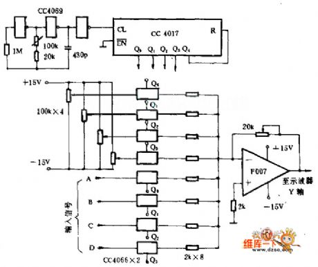
This display device uses the singleline oscilloscope to display the 4-channel continuous signal to compare the time relationship of different signals.
CC4017 is the oscillator and counter, it forms the 4 beats circuit and controls 4 pairs of analog form to connect them in turn. You can add the adjustable DC level and the one channel signal to each pair of analog switch, the signal will be mixed by the adder which is composed of the operational amplifier, and issent to the Y-axis of oscilloscope. Because the signals correspond to the different DC levels, so the oscilloscope can separate the 4 channels of signals.
(View)
View full Circuit Diagram | Comments | Reading(859)
The 90W, 15V, 6A switching voltage stabilization power supply circuit
Published:2011/5/19 18:31:00 Author:Christina | Keyword: switching, voltage stabilization, power supply
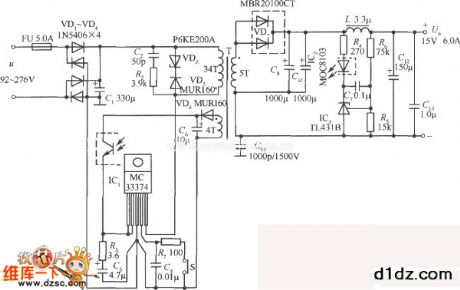
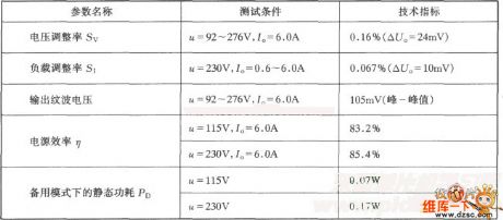
The 90W, 15V, 6A switching voltage stabilization power supply circuit which is composed of the MC33374 is as shown. This circuit uses the E28 type ferrite core, the primary coil and the feedback coil's wire diameter will not change, the turn numberis 34 turns and 4 turns, respectively. The secondary coil uses the φ0.8mm enameled double thread paratactic around wire. The core's air-gap is 0.56mm. The specifications of the power supply areas shown in the table:
The specifications of the power supply areas shown in the table:
(View)
View full Circuit Diagram | Comments | Reading(1099)
stable threshold voltage circuit
Published:2011/5/25 19:18:00 Author:Christina | Keyword: stable, threshold, voltage circuit
Figure: stable threshold voltage circuit (View)
View full Circuit Diagram | Comments | Reading(922)
RC Step-down circuit
Published:2011/5/18 19:16:00 Author:John
RC Step-down circuit is shown below.
(View)
View full Circuit Diagram | Comments | Reading(867)
Produced by six-inverter DC / DC conversion circuit
Published:2011/5/27 7:07:00 Author:John | Keyword: six-inverter
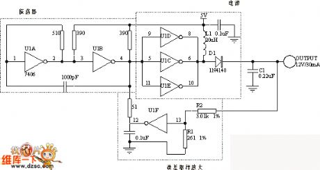
The circuit adjusts the voltage by controlling TTL switching threshold. U1A and U1B form the oscillator andtheoscillator'sswitching frequency is less than 1MHz. Output of oscillator drives three parallel inverters U1C, U1D and U1E. They can provide higher output current and output power. The internal output transistor, L1 and D1 form a standard boost converter. When the output is low, the current only flows through the inductor L1. When the output is higher, the energy stored in the inductor forces the anode of D1 to become higher. C1 conducts to charge D1.
(View)
View full Circuit Diagram | Comments | Reading(977)
battery car charger production with low cost and high reliability circuit
Published:2011/5/27 7:08:00 Author:John | Keyword: battery car charger
Currently, MC3842 is the most widely used and the earliest single-ended drive for directly driving switch MOS FET. MC3842 can not put a stable voltage. At the same time, it also has a load current control. Thus, MC3842 is often referred as current control type switch power supply drive. There is no doubt that the charger has the unique advantage, resulting from features of MC3842. Only very few external components are needed to achieve constant pressure output. And the charge current can be controlled at the same time. Especially, that MC3842 can directly drive MOS FETsubstantially increase the reliability of the charger.
(View)
View full Circuit Diagram | Comments | Reading(996)
Automatic wire counting machine circuit
Published:2011/6/8 9:37:00 Author:John | Keyword: Automatic wire counting machine
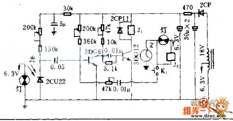
Photodiode 2CU22R accepts the optical signal uploaded to the machine. Such signals control sensitive relay to act through being amplified by the transistor. Then the alarm clock is driven to indicate the number of wires with the pointer.
(View)
View full Circuit Diagram | Comments | Reading(1058)
Numerical Control D. C. Regulated Power Supply Three
Published:2011/6/2 10:57:00 Author:Michel | Keyword: Numerical Control, D. C. , Regulated Power Supply, Three
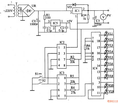
The numerical control D. C. power-supply circuits-fixedintroduced in the example uses dallastat and three-terminal tunable voltage regulatoion IC to regulate the voltage and adopts LED,voltmeter to indicate voltage.
Circuit's Work Principle
The numerical control D. C. regulated power supply circuit is composed of power converting circuit,+5V voltage regulation circuit,voltage regulation control output circuit and LED indication circuit and it is showed as the picture 5-22.The power converting circuit consists of mains transfomer,T,rectifier bridge,UR and filter capacitor,CO.The +5V voltage regulation circuit is composed of resistor,R1,capacitor,C1 and C2 and three-terminal voltage regulation IC,IC5.
(View)
View full Circuit Diagram | Comments | Reading(827)
Numerical Control D. C. Regulated Power Supply Two
Published:2011/6/2 10:54:00 Author:Michel | Keyword: Numerical Control D. C. Regulated Power Supply, Two
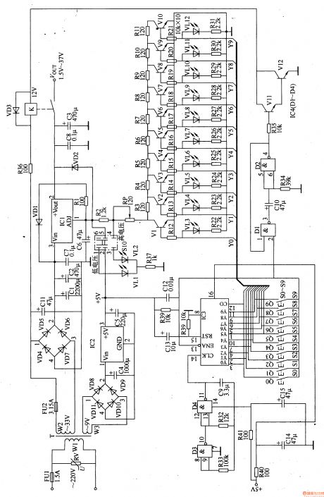
The numerical control D. C. regulated power supply circuit introduced in the example is controlled by tuch-button and digital integrated circuit.Its output voltage range is 1.5-37V divided into low voltage(1.5-15V) and high voltage(16.5-37V).
Circuit's Work PrincilpeThis circuit i scomposed of power supply input converting circuit,+5V voltage regulation circuit,functional mode indicating circuit and control circuit and it is showed as the picture 5-21.The power supply input converting circuit consists of fuse,FU1 and FU2,piezoresistor,RV,mains transformer,T and commutation diode,VD4-VD11.The +5V voltage regulation circuit is composed of filter capacitor,C4 and C5 and three-terminal voltage regulation IC,IC2.
(View)
View full Circuit Diagram | Comments | Reading(2775)
UC3842/UC3843 Isolation Single-end Flyback Switching Power Circuit
Published:2011/6/6 22:33:00 Author:Michel | Keyword: Isolation, Single-end, Flyback, Switching Power Circuit
Switching power supply has been widely used becauase of its advantages such as high efficiency, small volume. The traditional switch power supply uses voltage type pulse width modulation (PWM) technology, and recent years current-mode PWM technology has develpoed rapidly.Compared with voltage type PWM,current type PWM has better voltage and load adjustment rate.And the stability of system and dynamic characteristics also got significant improvement,especially its current-limiting and parallel current sharing ability make the control circuit simple and reliable.Current-mode PWM integrated controller has been industrialized,which pushes forward the small power switch power supply's development and application.Voltage-mode PWM controlling small power source has subsitituted current-mode PWM controlling small power power supply. (View)
View full Circuit Diagram | Comments | Reading(2386)
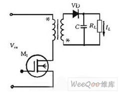
5V to 30V Booster Power Circuit of Gate Circuit
Published:2011/6/6 22:35:00 Author:Michel | Keyword: Gate Circuit, 5V to 30V, Booster Power Circuit
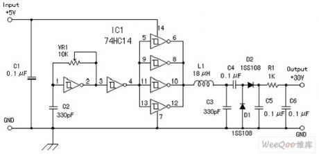
The 5V to 30V booster power circuit of gate circuit is showed as above. (View)
View full Circuit Diagram | Comments | Reading(1039)
Serial Adjustment Stabilized Voltage Supply Circuit
Published:2011/6/4 22:28:00 Author:Michel | Keyword: Serial Adjustment, Stabilized Voltage, Supply Circuit

The right picture is adjustable stabilized voltage power which uses crystal triode to output voltage.This circuit adjusts the output voltage by changing high-power crystal triode, tr1's voltage of load series. The output voltage,Vout,depends on A'svoltage,namely,Vref+VBE2.In the right formula,Vref(5.1V)is the voltage of voltage regulator diode,VBE2 is the emitter-to-base voltage of crystal triode Tr2,VR1 is variable resistor.Variable range of VR1 is 0~5kΩ so the variable range of output voltage is 7.6~12.8V.When VR1 sliding parts contact undesirable, the output voltage will be a minimum voltage. (View)
View full Circuit Diagram | Comments | Reading(621)
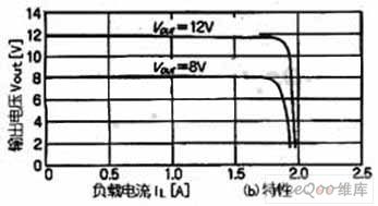
6V to 14V Booster Power Circuit of Discrete Device
Published:2011/6/6 23:38:00 Author:Michel | Keyword: Discrete Device, 6V to 14V, Booster Power Circuit
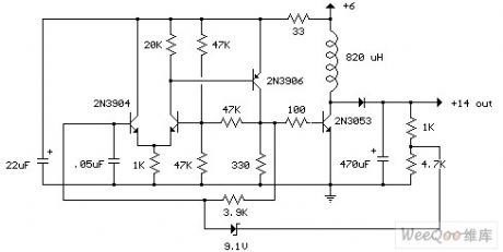
One schmitt trigger oscillator is used to drive the transistor and inductance energies stores in the inductance.The output voltage depends on load voltage and oltage regulator diode.This circuit's efficiency is about 80 %, and it also adopts the inductance with high Q value. (View)
View full Circuit Diagram | Comments | Reading(902)
Adjustable AC Power Supply Nine
Published:2011/5/20 2:50:00 Author:Michel | Keyword: Adjustable AC , Power Supply, Nine
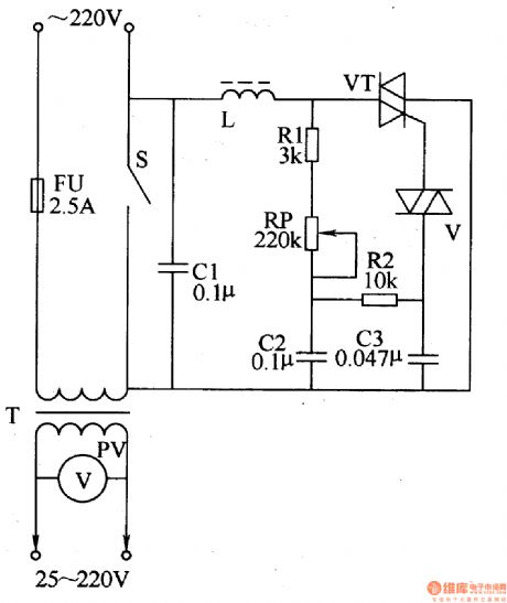
Alternating current power supply of different voltage grade is often used when we maintain household appliances.The alternating current power supply introudced in the example with the function of isolation can be used as maintenance power supply of household appliances such as color TV and its output voltage is 25-220V.
Circuit's Work Principle
This alternating current power supply circuit is composed of voltage regulation circuit and isolation output circuit and it is showed as the picture 5-62.The voltage regulation circuit consists of inductor,thyristor,VT,bidirectional trigger diode,V,resistor,R1 and R2,potentiometer,RP and capacitor C1-C3.
(View)
View full Circuit Diagram | Comments | Reading(2573)
Multifunction Charger Nine
Published:2011/5/19 9:29:00 Author:Michel | Keyword: Multifunction Charger Nine
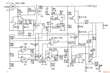
The multifunction charger introduced in the example uses switching power supply and has the functions of charging indication and discharging.Its maximum output current is about 300mA and it can charge nickel-pick,nickel-hydrogenlithium ion batteries.Circuit's Work PrincipleThis multifunction charger consists of oscillation suppression switching power supply circuit,protection circuit ,charging circuit ,discharging circuit,charging circuit and indication circuit and it is showed as the picture 5-71.The oscillation suppression switching power supply circuit is composed of diode ,VD1-VD6,switching tube V2,resistor,R3-R6,capacitor,C2 andswitching pulse transformer,T. (View)
View full Circuit Diagram | Comments | Reading(682)
| Pages:215/291 At 20201202203204205206207208209210211212213214215216217218219220Under 20 |
Circuit Categories
power supply circuit
Amplifier Circuit
Basic Circuit
LED and Light Circuit
Sensor Circuit
Signal Processing
Electrical Equipment Circuit
Control Circuit
Remote Control Circuit
A/D-D/A Converter Circuit
Audio Circuit
Measuring and Test Circuit
Communication Circuit
Computer-Related Circuit
555 Circuit
Automotive Circuit
Repairing Circuit