
power supply circuit
Index 26
Dual Output Power Supply +/-53V / 3A based on Transistors
Published:2013/3/18 21:21:00 Author:Ecco | Keyword: Dual Output Power Supply, +/-53V / 3A, Transistors
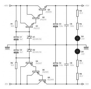
This is the circuit diagram of dual output power supply +/-53V / 3A based on transistors. This circuit has been designed for audio amplifier power supply requires a symmetrical + / -53 V (+ / -56 V maximum). The role of the circuit part presented here is to lower the voltage of both positive and negative lines of + / -65 V for non-hazardous + / -53 V for the amplifier, while allowing the current to 3 A in continuous operation.
The diagram above, based on the same principle as the previous circuit Dual supply + /-15V-based transistors, and is based on the use of common components. Differences of Dual supply + /-15V-based transistors, lies only in the number of transistors connected in cascade to allow high output currents while not requiring a zener diode of 10 W for output voltage stabilization. The main advantage of this type of configuration is to have a high current gain. The second point is not important in this case. Power dissipation in the ‘final’ two transistor Q3, and Q6 to 3 A output current, is about 36 W, which require a large heatsink. Transistors Q2 and Q5 is recommended fitted fin heat sink (for TO5 case).
(View)
View full Circuit Diagram | Comments | Reading(1619)
Single Power Supply with Soft Start
Published:2013/3/18 21:20:00 Author:Ecco | Keyword: Single Power Supply , Soft Start
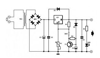
This Single power supply with soft start circuit which presented here has a simple concept, small power, smooth voltage. This power supply voltage is actually used for control kit K8003 © VELLEMAN, which allows to smooth ignition the exterior halogen spotlights (500 Watt) or interior spotlights (bathroom lighting for example), blackout is instantaneous. You must mount this circuit in the housing fully insulated and waterproof.
The circuit is based on the LM317, it is possible to varying the voltage between 1.25 V to 27 V depending on the voltage applied to the input (input voltage must be greater than 3 volts from the output circuit).
Increasing the value of the components (R and / or C) resulted in an increase in the rise time of 1.25 V to a preset voltage with P1. By the number shown in the component list, the time is ± 3 seconds for 10 V Usort.
(View)
View full Circuit Diagram | Comments | Reading(2521)
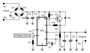
Isolated Power Supply +5 V to +15 V, 500 mA
Published:2013/3/18 21:19:00 Author:Ecco | Keyword: Isolated Power Supply , +5 V to +15 V, 500 mA
The Isolated Power supply +5 V to +15 V, 500 mA diagram represents a single control block, knowing that all are identical. It is truly classic, and is based on the use of common components. The Isolated Power supply +5 V to +15 V, 500 mA circuitdescribed belowis a “modification”that is designedtoaccommodateall the modulesona singlecircuit board.
Both terminals J1 and J2 (AC1 and AC1 ‘) is from secondary AC transformer. The AC voltage undergoes a wave rectification through four diodes D1 to D4 connected in a bridge, this voltage then filtered by capacitor C1. Values used in the diagram is 1000UF, may be increased to 2200 uF if the output ripple proved too big for your application. Voltage regulation is entrusted to the LM317 regulator IC, is slightly higher quality than its counterparts 78xx, but especially with the advantage that can be adjusted and able to work well over a wide output range. The capacitor C2 is optional, but it contributes significantly to the reduction of output ripple, therefore it is highly recommended. Two diodes D6 and D7 is also optional and only play a protective role is not always necessary at low currents. he output voltage is determined by the value of two resistors forming a voltage divider between output and ground, and whose midpoint is connected to the pin fitting U1.
(View)
View full Circuit Diagram | Comments | Reading(942)
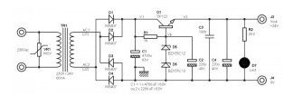
Dual Power Supply with Soft Power Switch
Published:2013/3/18 21:18:00 Author:Ecco | Keyword: Dual Power Supply , Soft Power Switch
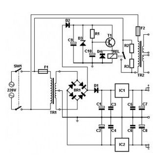
This power supply circuit brings together a dual polarity power supply and soft power to a power transformer (to supply a large amplifier for example) on the same board.
The regulator circuit is performed by a pair of 79xx and 78XX (XX = 12 to 24), if the current requirement does not exceed 200 mA, the heatsink is not needed here (but available in the printed circuit board). Tthis circuit part provides power to devices such as amplifiers (preamplifier, fans, the protection module etc. …).
Soft power for a large transformer is made by taking the series resistance of 100 ohms/10 watt or two resistors 47 ohm / 5 watts in the primary circuit, the resistance is shorted by the relay after ± 1.5 seconds. This avoids a sudden use of the current during power up. A Zener diode can be adjusted to allow the use of various voltage relay.
(View)
View full Circuit Diagram | Comments | Reading(1321)
24V / 2A DC Power Supply
Published:2013/3/18 21:17:00 Author:Ecco | Keyword: 24V / 2A DC Power Supply
The 24 volts power supply circuit is very simple. It uses a zener diodes and Darlington transistors type TIP122. Output voltage is set at 24 V with 2 amperes current output.
Lowering the voltage 230 V sector is provided by the transformer TR1, whose secondary voltage is 24 V. Available voltage after rectification and filtering is the order of 32 V to 34 V (depending on transformer and voltage).
Electrolytic capacitor C1 provides filtering rectified voltage to obtain the required output voltage. Its value depends on the maximum output current that you want to get, 4700 UF set here will allow you to simply filter 2 A output current. You can reduce it to 2200 uF if you dont need more than 1 A. The proposed circuit allows the implementation of one or two radial capacitors 2200UF-4700 UF, the choice is yours depending on the size of the capacitor that you can get.
The voltage stabilization is entrusted to a zener diode, which is supported by a Darlington transistor for output current capability greater (TIP122 transistor carries a collector current of 5 A continuous, so this is fine). In fact, if you look at the diagram, you find that there are two zener diodes instead of one. This choice allows you to change easily the output voltage by choosing other values of zener diodes. For this model, It used a 12 volt zener (BZX55C12) and a 13-V (BZX55C13), so that the output voltage is close to 24 V output current max. The output voltage depends a little on current consumption, this is quite normal for this type of scheme.
The power dissipated by the transistor Q1 is connected to the voltage difference that exists between its collector (regulated voltage of about 32 V) and its emitter (regulated voltage of 24 V), and supply output current (2 A max). Therefore, in 16 W at full capacity, which requires the use of cooling radiators in Q1.
(View)
View full Circuit Diagram | Comments | Reading(1477)
Mobile NiCd Charger
Published:2013/3/18 21:14:00 Author:Ecco | Keyword: Mobile NiCd Charger
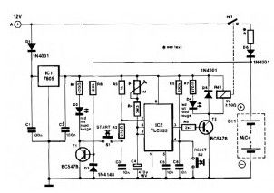
This mobile battery charger is designed primarily in order to give model enthusiasts the opportunity of charging their Nicad batteries from a car battery out in the open.
When the NiCd charger circuit is connected to the car battery, D2 lights only if the Nicad to be charged has been connected with correct polarity. For that purpose, the + terminal of the Nicad battery is connected to the base of T1 via R8. Because even a discharged battery provides some voltage, Ti is switched on and D2 lights.
Pressing thestart switchS1will have an effectonlyif ithas thecorrectpolarity. If so, the collector voltage of T1 is virtually zero so that monostable IC2 is triggered by S1. The output, pin 3, of this CMOS timer then becomes high, T2 is switched on and relay Rel is energized. Charging of the Nicad battery, via R5 and D6, then begins and charging indicator D4 lights. During the charging, C4 is charged slowly via Pl and R4. The value of these components determines the mono time of IC2 and thus the charging period of the Nicad battery. With values as shown in the diagram, that period can be set with P1 to between 26 and 33 min. Notice that this time is affected by the leakage current of C4; use a good-quality capacitor here. The charging can be interrupted with reset switch S2.
(View)
View full Circuit Diagram | Comments | Reading(1421)
Isolated Voltage Sensors for Monitoring Power Supply
Published:2013/3/18 21:13:00 Author:Ecco | Keyword: Isolated Voltage Sensors, Monitoring Power Supply
This is simple VCO ( voltage controlled oscillator) circuit , connected to your current instrumentation by an optoisolator, means that you can measure high voltages of your instrumentation more secure. The component values suit a 0 to 600 V input range (power dissipation in R1 and R2 set a limit on the input-voltage range). The circuit’s linearity is not an issue, because you can linearize its output in software.
The input voltage (VI), charges capacitor C1 until zener diode D1 conducts. Then, the zener diode triggers an “avalanche” circuit that discharges C1 into optocoupler Q1. After Cl discharges, the charging cycle repeats. C1 also averages the sensed-voltage level, which thereby provides noise immunity.
(View)
View full Circuit Diagram | Comments | Reading(830)
Simple LCD Power Supply
Published:2013/3/18 21:12:00 Author:Ecco | Keyword: LCD Power Supply
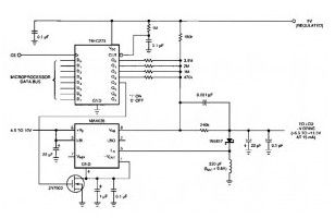
Laptop display commonly apply large screen Lcds, which generally will need a adjustable and a negative supply to ensure highest possible contrast. This circuit works with the system’s positive notebook battery supply and generates a digitally adjustable negative voltage to drive the large screen Lcd notebooks..
The following figure’s switching regulator generates a negative voltage by the notebook battery supply. The microprocessor data bus drives a 4-bit DAC( 74HC273 ), which in turn can vary the regulator output between 6.5 to 11.5 V. This arrangement enables a staircase of 16 possible voltages between these limits. The LCD power supply circuit implements the DAC by using the rail-to-rail output-drive capability of a 74 HC-series CMOS gate. A resistor divider network made by the 240-kO resistor, connected to the V filter capacitor as well as the resistors, is referenced to the 5 V supply control (the MAX635 regulator).
When the voltage at the VFB pin is greater than ground, the switching regulator turns on. The inductor dumps this energy into the – V filter capacitor. When the voltage at VFB is less than ground, the regulator skips a cycle. The MAX635 regulates the voltage at the junction of the resistor divider to 0 V. Thus, any resistor that the DAC connects to ground (logic 0) will not contribute any current to the ladder. Only the resistors that are at 5 V (logic 1) will be part of the voltage-divider equation.
The entire switching-regulator supply draws less than 150 uA. You can place the circuit in an even lower power mode by interrupting the ground pin. The high-current path is from the battery input through the internal power PMOSFET to the external inductor. Disconnecting the ground connection simply disables the gate drive to the FET and turns off the internal oscillator.
(View)
View full Circuit Diagram | Comments | Reading(986)
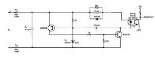
Switch Mode Voltage Regulator with 85% efficiency
Published:2013/3/18 21:11:00 Author:Ecco | Keyword: Switch Mode, Voltage Regulator, 85% efficiency
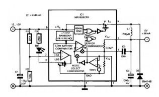
Switch Mode Power Supplies (SMPS) is now widely used in modern electronic equipment due to its compact design and high efficiency of about 80% or more. The switch-mode regulator circuit presented here has an efficiency of around 85%.
The circuit is quite simple thanks to the use of MAX638CPA 5V CMOS Step Down Adjustable Switching Regulator IC. With this IC input voltage of 12 to 16 Vdc converted into direct voltage 5VDC. You can see here is only using 9 additional external components to complete the circuit.
Resistors R1 and R2 are used to indicate when the battery voltage becomes low: as soon as the voltage on pin 3 becomes lower than 1.3 V, D1 lights. With values as shown for the potential divider, this corresponds to the supply voltage getting lower than about 6.5 V. The output of the IC is shunted by a simple LC filter formed by LI, C3 and D2.
The oscillator on board the IC generates a clock frequency of around 65 kHz and drives the output transistor via two NOR gates. The built-in error detector, the “battery low” indicator or the voltage comparator can block the clock frequency, which causes the transistor to switch off.
The MAX638CPA IC compares the output voltage of 5 V with a built-in reference (FET). Depending on the load, the FET will be switched on for longer or shorter periods. The maximum current through the FET is 375 mA, which corresponds with a maximum output current of 80 mA.
(View)
View full Circuit Diagram | Comments | Reading(840)
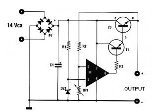
High Performance Gelled lead acid charger
Published:2013/3/18 21:10:00 Author:Ecco | Keyword: High Performance, Gelled lead , acid charger
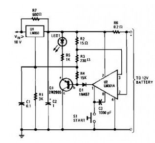
This high performance battery charger circuit allow quickly charges gelled lead-acid batteries, and automatically turns off at full charge. First, the charge current is held at 2 A, but as battery voltage rises, the current will decreases. When current falls to 150 mA, the charger automatically switches to a lower float voltage to keep from overcharging. When you hit full charge, transistor Q1 lights the LED to indicate that status.
(View)
View full Circuit Diagram | Comments | Reading(1028)
A simple variable power supply circuit with L200
Published:2013/3/18 21:09:00 Author:Ecco | Keyword: A simple , variable power supply
Variable power Supply scheme shown here is very simple, its used regulator IC L200 (ADJUSTABLE VOLTAGE AND CURRENT REGULATOR). L200 is a monolitthic IC for current and voltage programmable regulation. It has current limiting, power limiting, thermal shutdown, and over voltage protection.
Variable power supply based L200 for its output voltage is controlled by a variable resistor 10K. Output voltage range of values is from around 3 to 15 volts, and current range is about 10 mA minimum and a maximum of 2 amps. Exceeding current limit will reduce the output voltage to zero.
(View)
View full Circuit Diagram | Comments | Reading(1853)
Adjustable regulated power supply 3-30 V / 2.5 A
Published:2013/3/18 21:07:00 Author:Ecco | Keyword: Adjustable, regulated power supply , 3-30 V, 2.5 A
This Adjustable regulated power supply circuit uses voltage regulator LM723 IC which are already well known. IC LM 723 is designed to provide a voltage of 2-37 volt supply voltage with 150mA current, and this current is small indeed, but with the help of an external transistor can be achieved current up to 10 A, and in this circuit can provide voltage 3-30V and is limited to 2.5 A currnt with the help of TR2.
(View)
View full Circuit Diagram | Comments | Reading(1713)
DC power supply 3-30V 3-30V 3A stabilized
Published:2013/3/18 21:06:00 Author:Ecco | Keyword: DC power supply, 3-30V , 3A stabilized
This DC power supply circuit diagram is designed as an additional or as a permanent power supply for all general circuits based on a stable DC voltage between 3 and 30V provided that current consumption does not exceed 3A. Of course, this DC power supply can also be used to other purposes. By replacing the trimmer by a potentiometer, it can even be used as adjustable supply unit. A good quality heatsink must be used.
(View)
View full Circuit Diagram | Comments | Reading(1262)
Voltage reducer 24V to 12 V at 2.5 A
Published:2013/3/18 21:05:00 Author:Ecco | Keyword: Voltage reducer, 24V to 12 V , 2.5 A
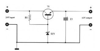
Thiscircuitisa voltagereducer24Vto12Vwithoutput current of2.5A,itcan adaptin avarious uses, it is suitableto be installedon atruckbecause ofall theelectricalcircuitsof car audio,radioandsomeother moderndevicesforcarsrequire12voltsupplyvoltage.
The use ofthis voltagereducercan also be expandedtothe CB transmission/receiver, this isdue tosupport ofcurrent2.5ampsmaximum.
(View)
View full Circuit Diagram | Comments | Reading(1044)
Battery charger indicator based LM393
Published:2013/3/18 21:00:00 Author:Ecco | Keyword: Battery charger indicator
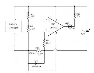
The circuit above willmakeyoursimplebatterychargerlook sophisticated. This circuit is a charging indicator forbatterycharger. Its usedtocheckwhether thebatteryis chargingornot.VoltagecomparatorLM393 ICis the heartofthis Battery charger indicator circuit.
D1LEDstays litwhenthere areat least 25milli-amps of currentwhich flowsto the battery. This circuit isdesignedspecifically for12Vbatterywith aload currentof1A.With a littlemodifying component values,load currentand voltagecan be changed.
(View)
View full Circuit Diagram | Comments | Reading(2541)
12 V Car battery charger based 7812
Published:2013/3/18 20:58:00 Author:Ecco | Keyword: 12 V , Car battery charger
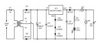
Below isa verysimplecircuitthat can be usedto charge12vcar battery. In this circuitthere isinstallationstocontrolthe charging currentand voltage. Thecircuit is based onthe circuitMC78T12ABTICfrom Freescale. ICis actually a7812with a TO-3packagewith a capacity of3A.
T1is atransformertoreducevoltageand thediodesD1andD2 performas arectifier.C1capacitoris to filterandthecapacitorC2 decoupling. The ground terminalofIC1is raisedto2.1Vusingthe diodesD3,D4andD5. Thus, theoutputofIC1is fed to14.1V(12+2.1).The battery is chargedthroughdiodeD6. D6 blocksthe flow ofreversecurrent from the batteryto the load circuit when AC poweris not available. MeterM1 showsthe charging currentand M2ofthe charge voltage.
(View)
View full Circuit Diagram | Comments | Reading(1821)
Flashing battery monitor
Published:2013/3/18 20:53:00 Author:Ecco | Keyword: Flashing battery monitor
Here is asimple battery monitor circuitin which theLEDwillcontinueflashinguntil battery voltageis above thelevel. TransistorsQ1andQ2arewiredasan astable multivibratorcircuit. Thisflashingbatterymonitorcircuitcan operatefroma variety ofvoltagesfrom6Vto12V.
Thevoltagelevelat whichanLEDstopsflashingcan be setby adjustingR4. When thea presetbatteryvoltagereachesthresholdflashingfrequencydecreasesandwhenthe voltagedrops belowthe threshold ofthe diodeD1LEDturnsOFF. This is usedtocompensate for changesinvoltage ofthe baseemitterQ1due the changes intemperature.
(View)
View full Circuit Diagram | Comments | Reading(942)
Solar panel battery charger
Published:2013/3/18 20:52:00 Author:Ecco | Keyword: Solar panel, battery charger
The solarbattery chargercircuit isnothing but adualcomparatorthat connects thesolar panelto the batterywhen thevoltage atthelatter terminalis lowand disconnected ifexceeding a certain threshold. Since itisonlybymeasuring thebattery voltage,it is especially intendedfor lead batteries, aelectrolyteliquid or gelled, thatadaptthebestofthisway.
The battery voltageseparatedbyR3before being fedtothe two comparatorsinIC2, When itis belowthe thresholddetermined bytheoutputofP2, IC2Bgoes highwhichalsocausesthe output ofIC2Chigh. T1saturationandrelayRL1on, allowingthe solarpaneltorechargingthe batteryvia theD3. When thebattery voltageexceedsthe threshold set byP1, When thebattery voltageexceedsthe threshold set byP1,the outputICAgoeslowas well asIC-C…and thereforecauses therelayoff,thus avoidingoverloadingwhen chargingthe battery. In orderthe thresholddeterminedby theP1andP2arestable,they aresuppliedwithan integratedregulatorIC, closelyseparatedfrom thevoltageofthe solarpanelthroughD2andC4.
(View)
View full Circuit Diagram | Comments | Reading(1051)
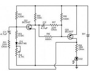
Car Nicd Battery charger
Published:2013/3/18 20:51:00 Author:Ecco | Keyword: Car Nicd , Battery charger
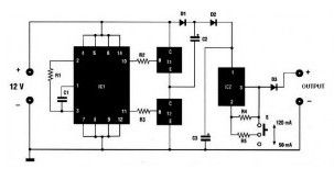
This is a car nicd battery charger circuitthat can chargeanyNi-Cdbatterybetween 4.8 and4.4 voltsfromaclassic12Voltscar battery.Thecharging currentis constantitcan beselected from the valuesof 50 to120mAbythe selectorS.
This feature is veryuseful formodel makingenthusiasts,forvideooperators,to those who usesmall appliancestransmissionandreceptionto all thosethat useNi-Cdbatteriesand needto rechargeorvoltagenetworkis not available.
(View)
View full Circuit Diagram | Comments | Reading(869)
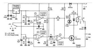
Automatic battery charger 14-15V input with 3A max current
Published:2013/3/18 20:50:00 Author:Ecco | Keyword: Automatic battery charger, 14-15V input , 3A max current
Automatic battery charger circuit is possible to realize a battery charger with excellent quality that allows it to recharge the 12 volt car battery and dry battery used in thealarm system. Operation is completely automatic, because it connects battery, battery charger will only charge the battery if it runs out, because it automatically disconnect the batteries fully charged. This device is supported by transformer with secondary voltage is 14-15 volts with a minimum of 3 Ampere current.
Theadjustmentof the trimmerTR1isawayyoudo,the outputof the battery charger, a voltage of about14.4voltswith no load.The maximum currentof3 Amperesfor distribution, it isthereforeadvisedto NOTtryto rechargebatterieswithaSuperiorcapacity 36Ah.
(View)
View full Circuit Diagram | Comments | Reading(1804)
| Pages:26/291 At 202122232425262728293031323334353637383940Under 20 |
Circuit Categories
power supply circuit
Amplifier Circuit
Basic Circuit
LED and Light Circuit
Sensor Circuit
Signal Processing
Electrical Equipment Circuit
Control Circuit
Remote Control Circuit
A/D-D/A Converter Circuit
Audio Circuit
Measuring and Test Circuit
Communication Circuit
Computer-Related Circuit
555 Circuit
Automotive Circuit
Repairing Circuit