
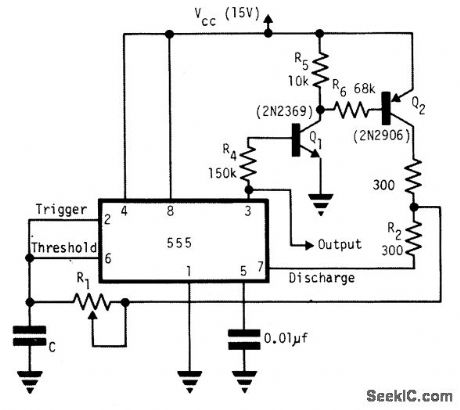
555 Circuit
Index 11
Yage Sedan V6 Engine Electronic Control System Circuit (the 1st)
Published:2011/7/18 2:57:00 Author:Felicity | Keyword: Yage Sedan, V6 Engine, Electronic Control System, Circuit, (the 1st)
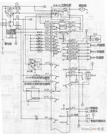
View full Circuit Diagram | Comments | Reading(844)
Yage Sedan 4-cylinder Engine Control System Circuit (the 1st)
Published:2011/7/18 3:02:00 Author:Felicity | Keyword: Yage Sedan, 4-cylinder Engine Control System, Circuit, (the 1st)
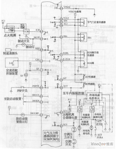
View full Circuit Diagram | Comments | Reading(833)
Yage Sedan 4-cylinder Engine Electronic Control System Circuit
Published:2011/7/18 3:06:00 Author:Felicity | Keyword: Yage Sedan, 4-cylinder Engine, Electronic Control System, Circuit
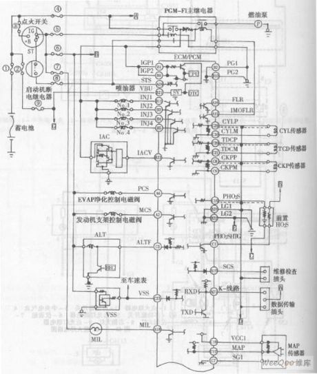
View full Circuit Diagram | Comments | Reading(876)
Linear Pulse Width Modulator circuit (555)
Published:2011/8/4 8:47:00 Author:nelly | Keyword: Linear, Pulse Width, Modulator
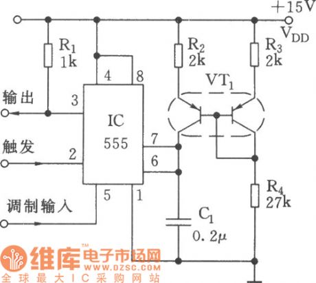
Linear Pulse Width Modulator circuit (555) (View)
View full Circuit Diagram | Comments | Reading(1678)
Alternately change polarity pulse width modulator circuit (555)
Published:2011/8/4 8:43:00 Author:nelly | Keyword: change polarity, pulse width, modulator
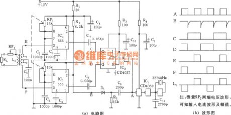
(a)circuit diagram (b)waveform
Note:measuring the voltage waveform at the two ends of PR2 can know the waveform and amplitude of input current. (View)
View full Circuit Diagram | Comments | Reading(1629)
60_Hz_CLOCK_OUTPUT_FROM_555
Published:2009/7/10 22:45:00 Author:May
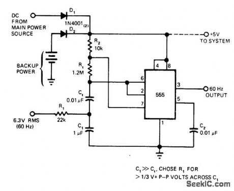
Basic 555 timer IC produces constant 60-Hz rectangular output for use as noninterruptible free-wheeling dock source. C1 introduces filtered 60-Hz power-line reference component across Ct at 2 V P-P. This signal overrides normal timing ramp of 555, causing it to act as amplifier or Schmitt trigger. When AC Iine power fails, Ct resumes normal function as timing capacitor for 60-Hz astable MVBR. Circuit can easily be adiusted for other reference frequencies.-W. G. Jung, Take a Fresh Look at New IC Timer Applications, EDN Magazine, March 20, 1977, p 127-135. (View)
View full Circuit Diagram | Comments | Reading(6255)
555_BEEP_TRANSFORMER
Published:2009/7/10 1:53:00 Author:May
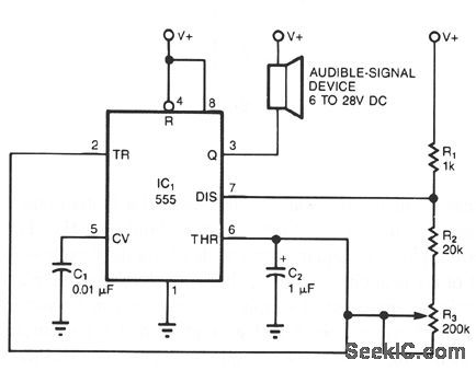
The simple circuit transforms the steady beep of an audible-signal device, such as a Mallory sonalert, into a distinctive warble or chirp. The value of C2 determines just what tone color you'll get. With the 1-μF value shown, the circuit produces a warble similar to the ring tone of an inexpensive phone. A 10-μF value produces a chirp similar to a truck's back-up alarm. One elaboration of this circuit would be to use the second section of a 555 timer to drive a piezoelectric transducer instead of a sonalert; that modification would vary the tone's pitch, as well as the chirp rate. (View)
View full Circuit Diagram | Comments | Reading(1529)
The ABS USB data, grouped instrument and ABS /traction control unit circuit of Buick-MPV (GL8)
Published:2011/7/20 1:51:00 Author:Borg | Keyword: grouped instrument, control unit circuit, Buick-MPV
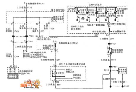
Figure 1. The ABS USB data, SP205, PCM, BCM, grouped instrument and ABS /traction control unit circuit of Buick-MPV (GL8)
(View)
View full Circuit Diagram | Comments | Reading(945)
SLIDE_SHOW_TIMER
Published:2009/7/9 1:34:00 Author:May
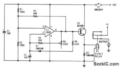
You can set the interval from about 5-30 seconds. A relay operates the slide-change mechanism. Op amp U1 forms a sort of Schmitt trigger. Resistors R1 and R2 bias the noninverting input at pin 3 of U1 to half the supply voltage. Feedback resistor R3 increases or reduces the bias to pin 3, depending on whether the output of U1 is high or low.When power is first applied to the circuit, C2 has a zero charge and the inverting input of the op amp is at a lower voltage than its noninverting input. When the output of U1 is high, C2 begins to charge through R5 and D1. It takes about one second for the charge on C2 to reach the same voltage as that at the noninverting input of U1. At that time, the output of U1 begins a negative swing.Because of the positive feedback through R3, the voltage at the noninverting input is reduced and the output becomes more negative. The voltage at the noninverting input is about 1/4 of the supply voltage, and C2 begins to discharge through the resistor bank. The timing is controlled by R6.The resulting pulses are fed to the base of Q1, configured as an emitter-following buffer stage, which is used to activate relay K1. Transistor Q1 is necessary because op amps usually have an output current in the 20-mA range, which is too low to activate the relay. (View)
View full Circuit Diagram | Comments | Reading(1318)
THERMISTOR_CONTROLLED_TIMER_
Published:2009/7/8 5:49:00 Author:May


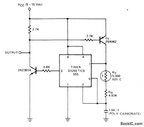


Thermistor and two transistors in charging network of 555 timer give outputfrequency that varies with temperature over 78°F range with accuracy of ±1 Hz. — Signetics Analog Data Manual, Signetics, Sunnyvale, CA, 1.977, p 731.
(View)
View full Circuit Diagram | Comments | Reading(1356)
CMOS_555_ASTABLE_GENERATES_TRUE_RAIL_TO_RAIL_SQUARE_WAVES
Published:2009/7/6 7:15:00 Author:May
A CMOS timer generates true square waves because, unlike the bipolar 555, its output swings from rail to rail. The component values shown give a frequency of about 400 Hz.
(View)
View full Circuit Diagram | Comments | Reading(1027)
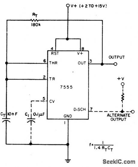
SQUARE_WAVE_GENERATOR_USING_A_555_TIMER
Published:2009/7/6 7:12:00 Author:May
A single timing resistor ensures that the output is a square (50% duty cycle) wave at at all frequency settings. (View)
View full Circuit Diagram | Comments | Reading(1451)
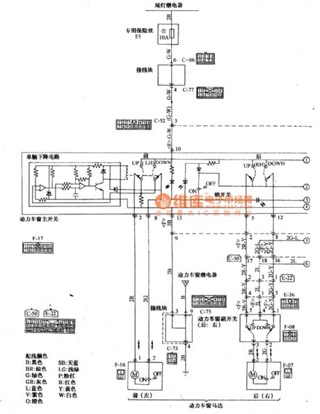
Mitsubishi Pajero light off-road vehicle power window wiring circuit diagram(Continued)
Published:2011/5/10 0:52:00 Author:Rebekka | Keyword: Light off-road vehicle , power window, Mitsubishi Pajero
Mitsubishi Pajero light off-road vehicle power window wiring circuit diagram(Continued) is shown as above. (View)
View full Circuit Diagram | Comments | Reading(2981)
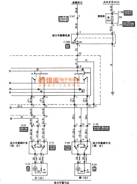
Mitsubishi Pajero light off-road vehicle power windows wiring circuit diagram
Published:2011/5/10 1:03:00 Author:Rebekka | Keyword: Mitsubishi Pajero , light off-road vehicle power
Mitsubishi Pajero (PAJERO) light off-road vehicle power windows wiring circuit diagram is shown as above.
Wiring color:B: black SB: light blue BR: brown LG: light green G: green P: pink GR: grey R: red L: blue Y: yellow V: purple W: white O: orange
(View)
View full Circuit Diagram | Comments | Reading(3477)
Mitsubishi Pajero light-weight off-road vehicle headlamp scrubber wiring circuit diagram
Published:2011/5/10 1:00:00 Author:Rebekka | Keyword: Mitsubishi Pajero , light-weight off-road vehicle
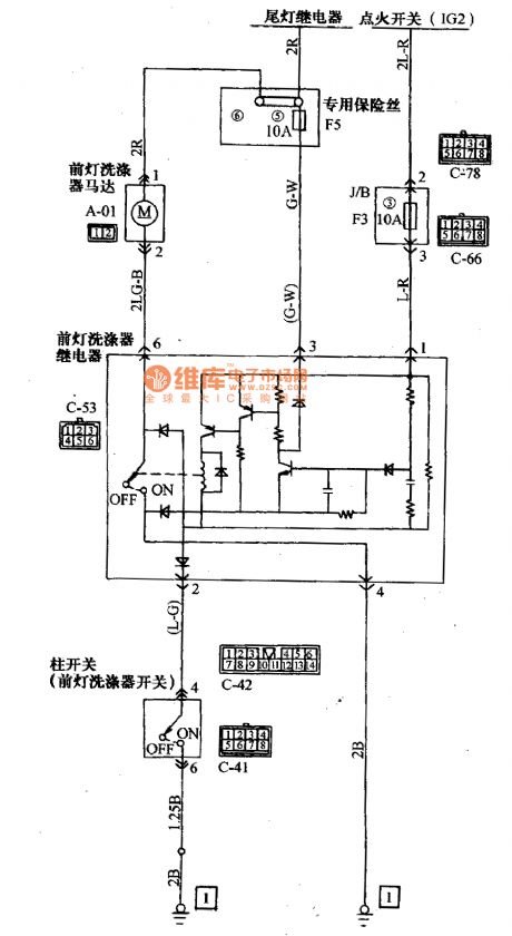
Mitsubishi Pajero light-weight off-road vehicle headlamp scrubber wiring circuit diagram is shown as above. (View)
View full Circuit Diagram | Comments | Reading(2097)
Mitsubishi Pajero light off-road vehicle before and after window wiper washing circuit diagram
Published:2011/5/10 0:58:00 Author:Rebekka | Keyword: Mitsubishi Pajero
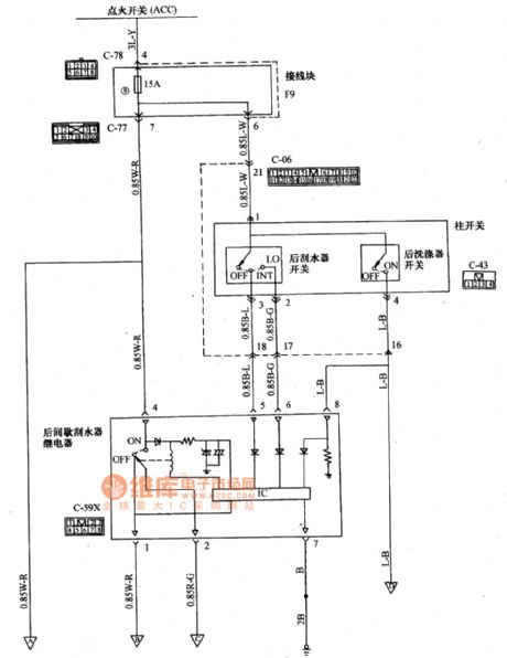
Mitsubishi Pajero light off-road vehicle before and after window wiper washing circuit diagram is shown as above. (View)
View full Circuit Diagram | Comments | Reading(1191)
Mitsubishi Pajero light off-road vehicles front and rear window wiper washing wiring circuit diagram
Published:2011/5/10 0:57:00 Author:Rebekka | Keyword: Mitsubishi Pajero, light off-road vehicles, wiper washing wiring
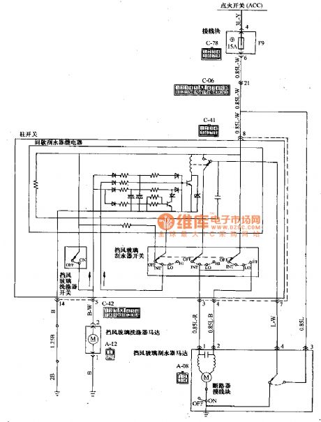
Mitsubishi Pajero light off-road vehicles front and rear window wiper washing wiring circuit diagram is shown as above. (View)
View full Circuit Diagram | Comments | Reading(2028)
555 Narrow pluse Generator Circuit
Published:2011/7/30 3:09:00 Author:Zoey | Keyword: 555, Narrow pluse, Generator, Circuit
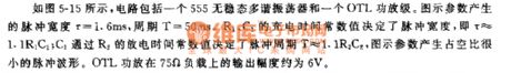
As shown in the figure 5-15, the circuit consists of a 555 astable multivibrator and an OTLPower Amplifier Stage. The parameter in the figure generates an pulse width r=1.6ms and a period T=50ms. The charge time constant determines the pulse width, that is , t≈1.1R1C1,and the pulse period T≈1.1R1C1 isdetermined by the charge time constant of R2. The parameter in the figure generates a pulse waveform that has a small duty cycle. When put on the 75 Ω load,the output magnitude of the amplifier OTLwill beabout 6V. (View)
View full Circuit Diagram | Comments | Reading(818)
Fixed Period pulse 555 Generator with a changeable Duty cycle
Published:2011/7/30 3:09:00 Author:Zoey | Keyword: Fixed Period pulse, 555 Generator , changeable Duty cycle
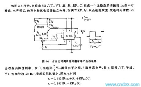

As shown in the figure 3-6,the astable multi-vibrator in the circuit consists of a 555 circuit, VT1,VT2, R1,R2,RP1 and C1.From the picture we can see that the capacitor C1 has a separate charge and discharge looped, the adjustment of RP1 will change its charge and discharge time constant instead of its oscillator frequency. Therefore, before C1 gets a 2/3 threshold level of VDD, pin 3willstayin high level, that is, during t1, VT2 will conduct, and VT1 will be saturated and conducted, thus, RVT1 presents a weak impedance, the charge time
t1=0.693(RVT1+R1+RP1left) C1
t2 =0.693(R2+RP1right) C1
T=t1+t2
=0.693((RVT1+R1+RP1) C1
DK=t1/T
then, adjust RP1 and the duty cycle can be limited in between 2%~98% with an unchanged period.
(View)
View full Circuit Diagram | Comments | Reading(1261)
555 Astable Oscillator Frequency and Duty Cycle Diagram for Quick Search
Published:2011/8/1 23:37:00 Author:Zoey | Keyword: 555 astable oscillator frequency, duty cycle diagram, quick search
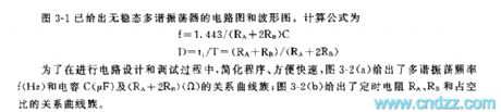
The circuit diagram and waveform of the astable multi-vibrator have been shown in picture 3-1.THey can be calculated according to the following formula:
f=1.433/(Ra+2Rb)C
D=t1/t=(Ra+Rb)/(Ra+2Rb)
In order to simplify, speed up, and convenience the procedure of debugging and designing the circuit, the relationship curve series between multi-vibrator’s oscillation and frequency f(Hz), capacitance C(μF) and (RA+2Rb)(Ω)has been illustrated in picture 3-2(a); The relationship curve series between time resistance, Ra, Rb and duty cycle has been shown in picture 3-2(b). (View)
View full Circuit Diagram | Comments | Reading(1079)
| Pages:11/47 1234567891011121314151617181920Under 20 |
Circuit Categories
power supply circuit
Amplifier Circuit
Basic Circuit
LED and Light Circuit
Sensor Circuit
Signal Processing
Electrical Equipment Circuit
Control Circuit
Remote Control Circuit
A/D-D/A Converter Circuit
Audio Circuit
Measuring and Test Circuit
Communication Circuit
Computer-Related Circuit
555 Circuit
Automotive Circuit
Repairing Circuit