
555 Circuit
Index 5
220V Solid State Flashing Lamp with 555
Published:2013/9/5 19:59:00 Author:lynne | Keyword: 220V Solid State Flashing Lamp with 555
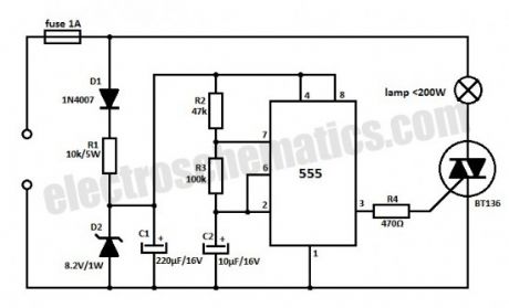
This 220V mains operated solid state flashing lamp circuit uses a 555 timer IC to control the ON and OFF times of a triac which controls power to the load. The power supply for the IC is obtained by half wave rectifier (D1), a stabilizer circuit (D2 and R1) and filter capacitor C1. The lamp stays ON for about 1 second and OFF for about 0.7 seconds. You can change these times by choosing other values for R2 and R3. (View)
View full Circuit Diagram | Comments | Reading(3605)
555 LED Flasher
Published:2013/9/4 20:02:00 Author:lynne | Keyword: 555 LED Flasher
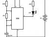
This is a small size led flasher built with the 555 timer IC that is powered from 2 x 1.5V batteries. The circuit can be used as a flashing metronome, dark room timer, memo-reminder or other similar applications.
The IC is connected as a astable multivibrator with a duty cycle of about 10%.In figure 1 the LED will be ON for a short period of time and OFF for a longer period. The duty cycle can be reversed if the LED is connected as shown in figure 2 but the battery consumption will also increase due to the fact that the LED will stay ON for a longer period of time. in figure 3 for a variable flash rate, replace the 220k pot with a 220k in series with a 22k resistor. And that is a simple 555 led flasher circuit. (View)
View full Circuit Diagram | Comments | Reading(1339)
555 Temperature Controller Circuit
Published:2013/9/3 20:04:00 Author:lynne | Keyword: 555 Temperature Controller Circuit
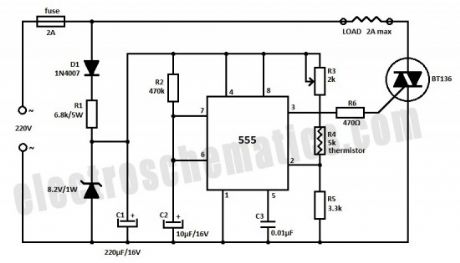
You can build a temperature controller circuit with the 555 IC together with a thermistor resistor divider. The advantage is that a well regulated power supply is not needed. The dividing network consists of adjustable resistor R3, thermistor R4 and R5.
When the thermistor temperature is below a set value the voltage at pin 2 of the 555 drops below 1/3 of Vcc. This turns on the triac controlled heater and also starts the timing cycle.
If the thermistor temperature rises above the set point before the end of the timing cycle the heater shuts off at the end of the timing period. Otherwise the heater continues to stay on.
Thermistors at different values can be used as long as R3 + R4 = 2 * R5 holds true at the desired temperature.
(View)
View full Circuit Diagram | Comments | Reading(2696)
555 Fast Reset Timer
Published:2013/8/22 20:05:00 Author:lynne | Keyword: 555 Fast Reset Timer
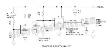

A common problem with on-delay timers is the timing capacitor reset. Typical timers (555 included) rely upon both complete power loss and finite elapsed time to assure that the timing capacitor is fully discharged. If this important detail is ignored, the timeout period is reduced and inconsistent. This 555 timer circuit resets almost instantly when Vcc drops below +10V. This circuit avoids the use of the 555 pin 4 reset feature that often causes more problems than it solves – this anomaly was previously documented in this article: Quirky 555 Timer Reset Function.
The initial application for this circuit was a reset timer in which the output was hard-wired across a reset pushbutton. The terminology is a little confusing because this is a reset timer that resets digital electronics, and the timer itself must reset instantly upon power loss by dumping the charge in the timing capacitor.
When digital components (including some Bluetooth stuff) are interconnected in automotive applications, initialization is sometimes an annoying problem that is complicated if both pieces of equipment do not have the same reset criteria (e.g. one component resets upon complete power loss, while another component resets when Vcc drops only briefly or slightly). In this application, a 50sec reset duration was found to be effective (I cannot provide more information because I was helping someone of a different language in a distant country).
More advanced software features provide a “warm” reset feature that automatically restores lost communications – in such a case, a reset timer is not required.
(View)
View full Circuit Diagram | Comments | Reading(1350)
555 Ignition Coil Driver
Published:2013/8/20 3:08:00 Author:lynne | Keyword: 555 Ignition Coil Driver
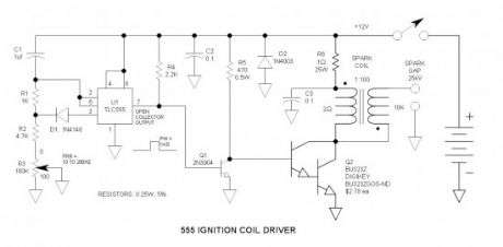
This ignition coil driver is a HOT one! From my recollection, it delivers a nastier spark than the legendary Ford Model T ignition coil. The circuit uses an inverted 555 oscillator that is coupled to an ON Semiconductor BU323Z Darlington transistor (350V, 10A) that drives a conventional inductive discharge ignition coil. In this topology, the inductive discharge voltage developed across the transformer primary is multiplied by the turns ration (factor of 100) to easily deliver a 25kV voltage to the spark gap. (View)
View full Circuit Diagram | Comments | Reading(3781)
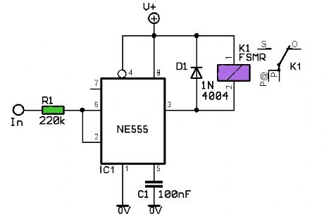
Momentary Switch with 555
Published:2013/3/27 4:20:00 Author:Ecco | Keyword: Momentary Switch , 555
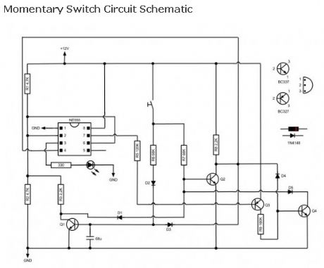
Based on NE555 this circuit turns on and off the IC output by a momentary switch. In other words it works as a mechanical latching relay, but the circuit backs to the start condition when you switch off the power supply. This feature is often required in automotive devices. No relay contacts are used, infact I connected the output to a led.
(View)
View full Circuit Diagram | Comments | Reading(1700)
555 Amplifier Circuit
Published:2013/3/4 21:26:00 Author:Ecco | Keyword: 555, Amplifier
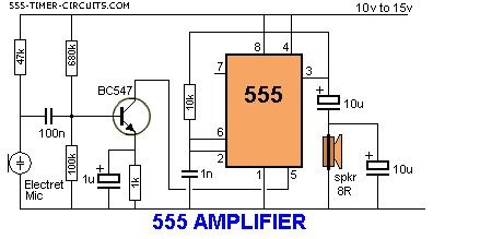
The 555 can be used as an amplifier. It operates very similar to pulse-width modulation. The component values cause the 555 to oscillate at approx 66kHz and the speaker does not respond to this high frequency. Instead it responds to the average CD value of the modulated output and demonstrates the concept of pulse-width modulation. The chip gets very hot and is only for brief demonstrations.
(View)
View full Circuit Diagram | Comments | Reading(2023)
Resistor quickly Estimating schematic with 555
Published:2013/1/23 2:17:00 Author:Ecco | Keyword: Resistor , quickly Estimating, 555
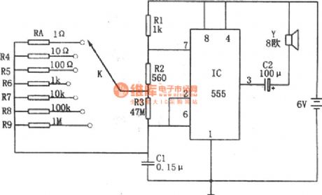
The core of circuit is a multivibrator composed of 555 and R1, R2, R3, Rx ( measured resistor ), C1, etc. The resistors R4 ~ R9 in circuit are the Estimating known resistors. The multivibrator output signals' period is T = 0.693 [ R1 +2 ( R2 + R3Rx / ( R3 + Rx ) ) ]. You can change the oscillation frequency by strobe switch K position, then the speaker issues different tone signals.
(View)
View full Circuit Diagram | Comments | Reading(1731)
PWM with 555
Published:2013/1/16 1:49:00 Author:muriel | Keyword: PWM , 555

View full Circuit Diagram | Comments | Reading(2481)
Timer with 555
Published:2013/1/16 1:47:00 Author:muriel | Keyword: Timer, 555

This circuit can be used to activate a relay for two or three minutes. Pressing the switch the relay will be activated. Changing the 1M resistor with a variable resistor you can vary the time. The 0.01 capacitor is important because it prevents any false triggering.
The circuit will work OK with 6 Volts without any modification. If you want to use 9 or 12 Volts, you need to change the relay with a 9V or 12V relay. Using this circuit with 120 VAC is not recommended, however, using the right parts and the right isolation, will be not a problem.
The aplications for this circuit may vary, for example: Bouce-free switch, A three-minutes light to walk thru a dark area, A timer-activated faucet to save water, etc. Any project that needs only a few minutes of power will be perfect for this circuit. Ever if you have an old microwave with the broken electronic control, you can replace it with this timer (using the right hi-current relay). (View)
View full Circuit Diagram | Comments | Reading(2109)
555 astable
Published:2013/1/10 22:01:00 Author:muriel | Keyword: 555 astable

View full Circuit Diagram | Comments | Reading(0)
555 Monostable
Published:2013/1/10 22:01:00 Author:muriel | Keyword: 555 Monostable

View full Circuit Diagram | Comments | Reading(1711)
555 timer
Published:2013/1/10 22:00:00 Author:muriel | Keyword: 555 timer

View full Circuit Diagram | Comments | Reading(1417)
VCS using 555 Timer
Published:2012/11/29 0:35:00 Author:muriel | Keyword: VCS using 555 Timer

View full Circuit Diagram | Comments | Reading(2790)
Pulse position modulating circuit with 555 time-base circuit
Published:2012/11/7 19:55:00 Author:Ecco | Keyword: Pulse position modulating , 555, time-base circuit
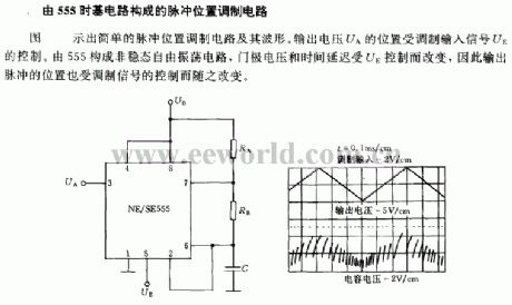
The figure illustrates a simple pulse -position modulation circuit and its waveform. The position of output voltage UA is controlled by the modulation input signal UE. 555 constitute a non - steady-state free oscillation circuit, and the gate voltage and time delay is changed by the UE control, therefore the position of the output pulses is controlled by the modulation signal.
(View)
View full Circuit Diagram | Comments | Reading(1723)
555 timer Mono stable (one shot) circuit
Published:2012/10/23 20:20:00 Author:muriel | Keyword: 555 timer , Mono stable, one shot
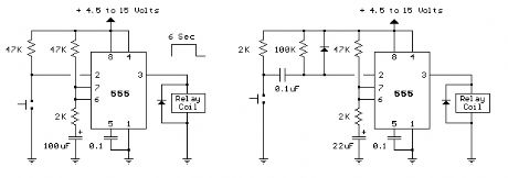
The two circuits below illustrate using the 555 timer to close a relay for a predetermined amount of time by pressing a momentary N/O push button. The circuit on the left can be used for long time periods where the push button can be pressed and released before the end of the timing period. For shorter periods, a capacitor can be used to isolate the switch so that only the initial switch closure is seen by the timer input and the switch can remain closed for an unlimited period without effecting the output.
In the idle state, the output at pin 3 will be at ground and the relay deactivated. The trigger input (pin 2) is held high by the 100K resistor and both capacitors are discharged. When the button is closed, the 0.1uF cap will charge through the button and the 100K resistor which causes the voltage at pin 2 to move low for a few milliseconds. The falling voltage at pin 2 triggers the 555 and starts the timing cycle. The output at pin 3 immediately moves up to near the supply voltage (about 10.4 volts for a 12 volt supply) and remains at that level until the 22 uF timing capacitor charges to about 2/3 of the supply voltage (about 1 second as shown). Most 12 volt relays will operate at 10.4 volts, if not, the supply voltage could be raised to 13.5 or so to compensate. The 555 output will supply up to 200mA of current, so the relay could be replaced with a small lamp, doorbell, or other load that requires less than 200mA. When the button is released, the 0.1uF capacitor discharges through the 100K and 2K resistors. The diode across the 100K resistor prevents the voltage at pin 2 from rising above the supply voltage when the cap discharges. The 2K resistor in series with the 22uF cap limits the discharge current from pin 7 of the timer. This resistor may not be necessary, but it's a good idea to limit current when discharging capacitors across switch contacts or transistors. (View)
View full Circuit Diagram | Comments | Reading(2597)
555 overvoltage indication circuit
Published:2012/10/16 21:54:00 Author:Ecco | Keyword: 555, overvoltage indication
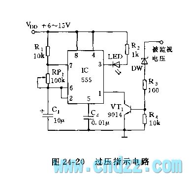
As shown in Figure 24-10, 555, R1, RP1 and C1 form astable multivibrator, but its ground pin is connected to c pole of detection transistor. When the monitored voltage exceeds set value, DW is breakdown, VT1 is saturated and turned, then 555 starts oscillation, LED light flashes. VT1 can also reduce the static power dissipation of 555. 555 oscillation frequency can be adjusted between 1 ~ 20Hz, and RP1 can be used to select the flashing number of LED.
(View)
View full Circuit Diagram | Comments | Reading(1894)
555 program controller circuit
Published:2012/10/16 21:35:00 Author:Ecco | Keyword: 555, program controller
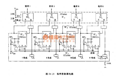
As shown in 24-10, it uses four 555 circuits which respectively form different timing monostable circuit, and they are concatenated cycle triggers. IC7 is timed and set by trigger monostable circuit composed of C4069's hex inverter. IC6 is four 2 -input AND gate; IC5 (CC4044) is four RS latch. When the start button is pressed, IC1 sets.
(View)
View full Circuit Diagram | Comments | Reading(1547)
Pulse generator circuit with 555
Published:2012/9/27 21:33:00 Author:muriel | Keyword: Pulse generator, 555
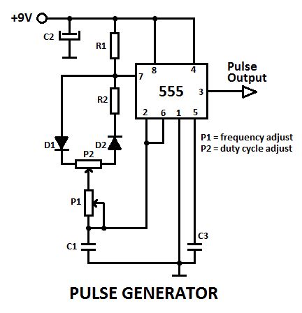
This is a pulse generator with adjustable duty cycle made with the 555 timer IC. The circuit is an astable multivibrator with a 50% pulse duty cycle. The difference from the standard design of a 555 timer is the resistance between pins 6 and 7 of the IC composed of P1, P2, R2, D1 and D2.The diodes D1 and D2 set a definite charging time for C1 which produces a 50% duty cycle in a normal case. The duty cycle (n) is dependent on P1 and P2 in the following manner:
n = 1 + P2/P1
If P2 = 0 (n = 100%) then the frequency can be approximately calculated with the following formula:
f = 0.69/((2*P1 + P2 + 4.7kΩ)*C1)
Pulse generator circuit diagram
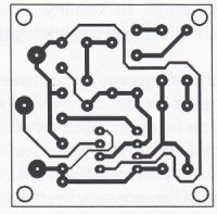
Printed circuit layout of the pulse generatorComponents ListC2 = 10µFC3 = 0.1µFR1 = R2 = 4.7KD1 = D2 = 1N4148IC = 555C1, P1 and P2 must be calculated (View)
View full Circuit Diagram | Comments | Reading(6566)
IC 555 Design Note
Published:2012/9/25 0:59:00 Author:muriel | Keyword: 555,Timer IC
The popular Timer IC 555 is extensively used in short duration timing applications. IC 555 is a highly stable integrated circuit functioning as an accurate time delay generator and free running multivibrator. But one of the serious problem in 555 timer design is the false triggering of the circuit at power on or when voltage changes. The article describes how IC555 is designed perfectly to avoid false triggering.
Functional aspects of pins
Trigger Pin 2
Usually pin2 of the IC is held high by a pull up resistor connected to Vcc. When a negative going pulse is applied to pin 2, the potential at pin 2 falls below 1/3 Vcc and the flip-flop switches on. This starts the timing cycle using the resistor and capacitor connected to pins 6 and 7.
Reset pin 4
Reset pin 4 can be controlled to reset the timing cycle. If pin 4 is grounded, IC will not be triggered. When pin4 becomes positive, IC becomes ready to start the timing cycle. Reset voltage is typically 0.7 volts and reset current 0.1 mA. In timer applications, reset pin should be connected to Vcc to get more than 0.7 volts.
Control Voltage pin 5
Pin5 can be used to control the working of IC by providing a DC voltage at pin5. This permits the control of the timing cycle manually or electronically. In monostable operation, the control pin5 is connected to ground through a 0.01 uF capacitor. This prevents the timing interval from being affected by AC or RF interference. In the Astable mode, by applying a variable DC voltage at pin 5 can change the output pulses to FM or PWM.
Threshold pin 6 and Discharge pin 7
These two inputs are used to connect the timing components- Resistor and Capacitor. The threshold comparator inside the IC is referenced at 2/3 Vcc and the trigger comparator is referenced at 1/3 Vcc. These two comparators control the internal Flip-Flop of the circuit to give High or Low output at pin 3.When a negative going pulse is applied to pin 2, the potential at pin2 drops below 1/3 Vcc and the trigger comparator switches on the Flip-Flop. This turns the output high. The timing comparator then charges through the timing resistor and the voltage in the timing capacitor increases to 2/3 Vcc.( The time delay depends on the value of the resistor and capacitor. That is, higher values, higher time).When the voltage level in the capacitor increases above 2/3 Vcc, the threshold comparator resets the Flip-Flop and the output turns low. Capacitor then discharges through pin 7.Once triggered, the IC will not responds to further triggering until the timing cycle is completed.
The time delay period is calculated using the formula T= 1.1 Ct Rt. Where Ct is the value of Capacitor in PF and Rt is the value of Resistor in Ohms. Time is in Seconds.
How to eliminate false triggering?
The circuit diagram shown below is the simple monostable using IC 555. To eliminate the false triggering resistor R1 and Capacitor C1 are connected to the reset pin 4 of the IC. So the reset pin is always high even if the supply voltage changes. Moreover capacitor C3 connected close to the Vcc pin 8 acts as a buffer to maintain stable supply voltage to pin 8. Using this design, it is easy to avoid false triggering to a certain extent.
555 Monostable circuit
(View)
View full Circuit Diagram | Comments | Reading(2289)
| Pages:5/47 1234567891011121314151617181920Under 20 |
Circuit Categories
power supply circuit
Amplifier Circuit
Basic Circuit
LED and Light Circuit
Sensor Circuit
Signal Processing
Electrical Equipment Circuit
Control Circuit
Remote Control Circuit
A/D-D/A Converter Circuit
Audio Circuit
Measuring and Test Circuit
Communication Circuit
Computer-Related Circuit
555 Circuit
Automotive Circuit
Repairing Circuit