
555 Circuit
Index 21
555 Symmetrical wave Multi-vibrator
Published:2011/7/4 22:58:00 Author:Zoey | Keyword: 555 Multi-vibrator, Symmetrical wave
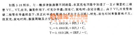
As shown in the figure 3-18, this multi-vibrator has added a positive bias triode VT1. With the positive bias effect of R2, VT1 can be fully conducted; but as soon as C1 discharges, it will not be conducted. As the switch pipe VT1 and Germanium diode is in the state of conduction, the positive conduction resistance is weak, so it has little effect on charge and discharge time constant. The charge time, discharge time, oscillation period and duty cycle can be calculated by following formula:
T1=0.693(R1+RP1)•C1
T2=0.693(R1+RP1)•C1
T=0.693(2R1+2RP1)•C1
D=T2/D=50%
Another merit of this circuit is, the load change has little effect on voltage output, duty cycle and oscillation frequency.
Figure 3-18 Multi-vibrator that can output symmetrical wave
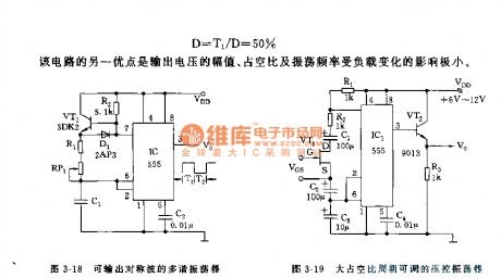
Figure 3-19 Voltage-controlled oscillator with an adjustable duty cycle period
(View)
View full Circuit Diagram | Comments | Reading(2154)
555 Power Supply Circuit that Changes from Single-supply to Dual-supply
Published:2011/7/5 0:11:00 Author:Zoey | Keyword: 555 Power Supply Circuit, Single-supply, Dual-supply

As shown in the figure3-8, the astable multi-vibrator consists of a 555, R1 and C2and its oscillation frequency is about 20kHz. As both the charge and discharge time constant are R1C2, the duty cycle is 50%. After the 20kHz pulse wave output have been filtered by D1, C3 and D2, C4 respectively, dual power supply ±EDDis output.
The application of dual time base helps load current to reach 50mAeven more.
(View)
View full Circuit Diagram | Comments | Reading(957)
555 Voltage-controlled Oscillator with an Adjustable Duty Cycle Period
Published:2011/7/5 0:10:00 Author:Zoey | Keyword: 555 Voltage-controlled Oscillator, Adjustable Duty Cycle Period
The voltage-controlled oscillation circuit has been shown in picture3-19. 555, R1, R2, C1~C3 and VT1 constitute a voltage-controlled multi-vibrator. As a voltage-controlled resistance, JFET can change the impedance between D/S. The coupling capacitance of D and S is used to eliminate the effect of other direct voltage on JFET. Timing capacitance of C1 and C2 should be selected as large as 10 times of C3.
Advantage of this circuit is that, an adjustable and changeable resistance can be formed by changing VGS, so as to obtain a large duty cycle and a changeable period.
(View)
View full Circuit Diagram | Comments | Reading(1153)
555 Low power consumption Monostable circuit
Published:2011/7/4 23:58:00 Author:Zoey | Keyword: Low power consumption, Monostable, circuit
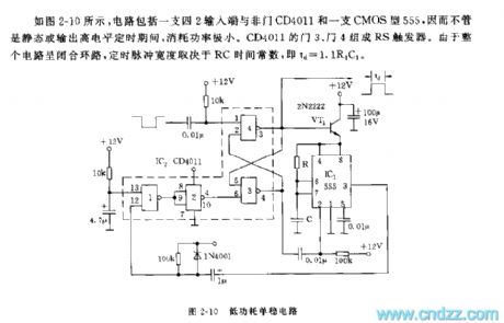
As shown in the picture 2-10, the circuit is composed of a four-two input terminal, a non-pin CD4011 and a CMOS-type 555, therefore, no matter in a stable state or in a state of outputting high-level pacification, it consumes little power. Pin 3 and pin 4 of CD4011 constitute an RS trigger. As the whole circuit is a closed loop, the time pulse width is determined by RC’s time constant, that is, td=1.1R1C1.
Picture 2-10 Low power-consuming Single stable circuit (View)
View full Circuit Diagram | Comments | Reading(1094)
Four Basic Circuits of 555 Monostable Trigger
Published:2011/7/5 Author:Zoey | Keyword: Basic Circuits, 555 Monostable Trigger
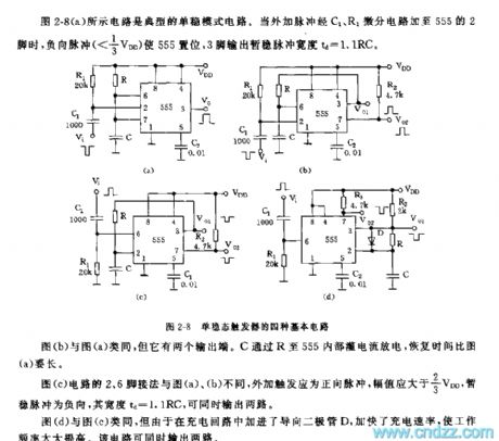
The circuit in the picture 2-8(a) is a typical monostable circuit. When external pulse is added to pin 2 of 555 via differential circuit C1 and R1, positive pulse will force 555 to set, temporarily stable pulse width that pin 3 outputs td is 1.1 RC.
Circuit in picture (b) has two output terminals. C discharges through R, and it takes longer for it to recover than that of (a).
Pin 2 and 6 in circuit of picture (c) joint a positive pulse, temporarily stable pulse is negative and the width is 1.1RC. They can output two circuits simultaneously.
Circuit in picture (d) has a faster charge ratio and higher work efficiency and can output two circuits simultaneously
(View)
View full Circuit Diagram | Comments | Reading(1645)
555 Linear Voltage/Frequency Converter circuit Four
Published:2011/7/4 23:57:00 Author:Zoey | Keyword: 555 Linear Voltage, Frequency Converter, circuit
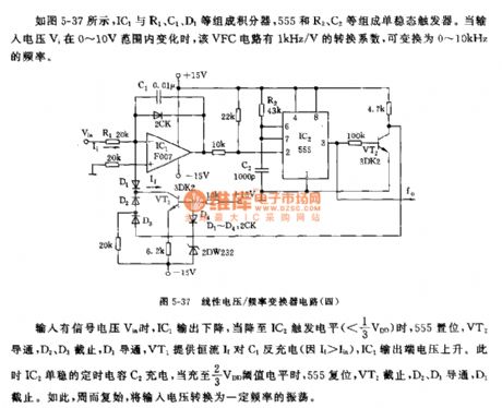
As shown in the picture5-37, IC1, R1, C1 and D1 constitute an integrator, 555, R2 and C2 constitute a monostable trigger, if input voltage Vi ranges from 0 to 10V, VFC circuit will have a conversion factor of 1kHz/V,which can be converted to frequency of 0~10kHz.
When signal voltage Vin is available, IC1 output will decline, andas soon asit declines to trigger level of IC2(<1/3VDD), 555 will set, VT2 will conduct,D2 and D3 will cease to work, D1 will conduct, VT1 will offer constant current to discharge to C1(If>Iin),output voltage on IC1 output terminal will rise. Then, monostable time capacitor C2 charges, when capacitance reaches to 2/3 VDD threshold level, 555 will reset, VT2 will cease to work, D2 and D3 will conduct, and D1 will cease to work. Therefore, move in cycles, voltage input is converted to oscillation that has various frequencies.
(View)
View full Circuit Diagram | Comments | Reading(1118)
555 Multivibrator Circuit
Published:2011/7/8 9:49:00 Author:Robert | Keyword: Multivibrator
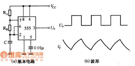
By using the 555 time-base circuit it can make up many kinds of self-excited multivibrator and its basic circuit is shown in picture a. When the circuit is firstly connected to the power, the C has not been charging in time, the 555 circuit's pin 2 is at low voltage level. This makes its pin 3 output high voltage level. When the C is in the status of Vc≥Vcc, which is charged by the power through RA and RB, the pin 3 output port would be changed from high voltage level to low voltage level. And the capacitor C would discharge through the RB and internal circuit's discharging switch tube. When it is discharged to Vc≤Vcc, the output port would be changed from low voltage level to high voltage level again. At this time the capacitor would be charging again. This process would cycle to proceed and it would form the self-excited oscillation. The picture (b) shows the waveform of voltage on the output port and capacitor C. (View)
View full Circuit Diagram | Comments | Reading(1378)
555 Time-Base Circuit Internal Structure Circuit
Published:2011/7/8 21:25:00 Author:Robert | Keyword: Time-Base, Internal, Structure
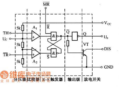
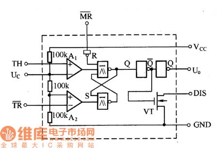
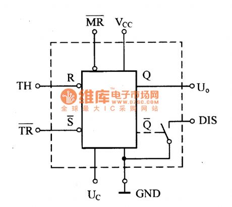
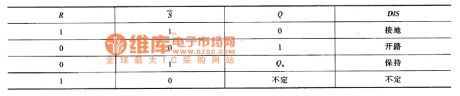
The 555 time-base circuit is divided into two categories which are TTL type and CMOS type. The picture shows the TTL type circuit's internal structure circuit. From the picture we notice that it is made up of voltage divider, comparator, R-S trigger, output stage and discharging switch and so on. The comparator's main function in the circuit is to compare the input voltage to the reference voltage formed by the voltage divider. And it would show the comparing result by outputing high voltage level 1 or low voltage level 0 in its output port. The 555 circuit's R-S trigger is made up of two NAND gates with cross connection. In order to reset the R-S trigger to zero directly, the trigger is lead to a MR port. It could simply set the MR port to low voltage level 0 , the trigger would be set to zero immediately which means Q=0=Uo, no matter what original status the trigger has and no matter what signal the trigger's input port is added. So the MR port is also known as the total-reset port. (View)
View full Circuit Diagram | Comments | Reading(1483)
555 bumper cars circuit
Published:2011/6/13 7:53:00 Author:nelly | Keyword: bumper car
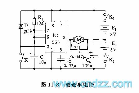
IC adopts ambipolar time base circuit 555, its load current can reach 200mA, it can drive toy motor directly. K1, K2 are toggle switch, when the car moves, K1, K2 are closed, due to 2 foot is high level, 3 foot is low level, the motor terminal's voltage is about 3V(the left is negative, the right is positive), the motor is positive turning, the car moves forward; when the car meets the object, the humper K is butted, 2 foot is connected to ground, the circuit is set, the output turns to high level(about 6V), the motor terminal's voltage is still 3V, but the motor is negative turning, the car gets back. Due to the action of car's reverse wheel, it is moving back and turning. After the circuit is set, C1 is charged by R1, when C1's voltage is charged to more than 6 foot's threshold level 2/3 VDD=2/3(E1+E2)=4V, then the monostable circuit's temporal stability is ended, the car recovers to the former state and moves forward again.
(View)
View full Circuit Diagram | Comments | Reading(1798)
555 electric bumper cars control circuit
Published:2011/6/13 8:12:00 Author:nelly | Keyword: electric bumper car, control

The monostable timing circuit is composed of time base circuit 555 and R1, C1. When the power supply switch SA1, SA2 are connected, C1 is charged by R1, after 1s, C1's voltage is charged to 2/3 VDD(4V), 555 is in reset state, 3 foot's output is low level, the driving tube VT1 is turned on, the closed circuit is made of motor M and voltage source U1, then the motor M obtains the electricity, M turns into normal positive turning, the electric car moves forward straightly.
When the electric car meets barrier, C1's electricity is diacharged, 555's 2 foot is low level, 555 is set, its 3 foot turns to high level.
(View)
View full Circuit Diagram | Comments | Reading(2059)
555 electric rolling circle game machine circuit
Published:2011/6/13 8:44:00 Author:nelly | Keyword: electric rolling circle, game machine
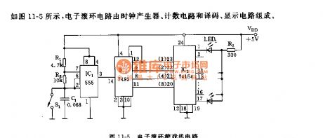
As shown in the figure 11-5, the electric rolling circle circuit is composed of clock generator, counting circuit and coding, display circuit.
The astable multivibrator is composed of 555 and R1, R2, C1, the oscillation frequency f=1.44(R1+2R2)C1, it is about 1000Hz. As IC2's counting clock, its output is added to 14 foot. IC2(74LS93)is TTL type four-bit binary system counter, its 8-4-2-1 code output is added to IC3(74LS154), IC3 is 4-line to 16-line encoder, its 16 output lines take 1 from 16 according to IC2's binary number, and it is low level in order, the circinal 16 LEDs LED1~LED16 are lighted in order, they are chasing rolling ball-shaped.
(View)
View full Circuit Diagram | Comments | Reading(1365)
555 automatic reset electric shock protector circuit
Published:2011/6/21 6:43:00 Author:nelly | Keyword: automatic reset, electric shock, protector
The tube is connected to 555's trigger terminal 2 foot, ordinarily, VT1 tube cuts off, 2 foot is high level. A monostable circuit is composed of 555 and R2, C5. When VT1 tube is turned on, 2 foot level is lower than trigger level 1/3 VDD, 555 is set, 3 foot turns into high level, LED lights, relay J pulls in, the AC power supply is cut off. 555 internal discharge tube is open, C5 is charged by R2, when C5's voltage is higher than 2/3 VDD threshold level, the circuit is reset, 3 foot turns to low level, J releases, it recovers to transmit electricity. After trigger monostable, the delay time td=1.1R2C5, the figured parameter's delay time is about 10s. When the circuit has electric shock, due to VT1 tube is turned on, so 555 is in trigger delay state all the time, J can not release, the power supply is cut off.
(View)
View full Circuit Diagram | Comments | Reading(1928)
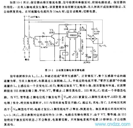
555 DC regulated power supply protection device circuit
Published:2011/6/21 6:22:00 Author:nelly | Keyword: DC regulated power supply, protection device
The protector consists of depressurization regulated power supply, VDD=+(5~12)V, it depends on which voltage stablizing unit is adopted by IC1. The controllable monostable delay circuit is composed of IC2(555) and C4, R3. Ordinarily, due to J1-1 is short connected, when the load is normal, 4 foot level is higher than 1V; when it is short circuit, 4 foot is low level(<0.6V), 555 is in forced reset state, 3 foot is low level, J pulls in, J1-1 is cut off quickly, the short circuit's load is turned off. At the same, J3-3, J2-2 contacts are turned on, the audio frequency feedback type oscillator which is made of VT1, VT2, C6, C7, R6 obtains electricity and oscillates, it sends out about 1000Hz audio. J3-3 is connected, C4 is charged, then 555's 2 foot level is lower than 1/3 VDD, 555 is set, J releases, J1-1 normally closed contact is turned on again.
(View)
View full Circuit Diagram | Comments | Reading(1420)
555 touching SCR zero-crossing switch circuit(2)
Published:2011/6/14 3:04:00 Author:nelly | Keyword: touching SCR, zero-crossing switch
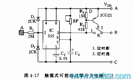
The monostable timing circuit consists of the 555 and D1,D2,RP,C2. The inductive signal makes the 555 reset when thebody touches the metal disc A. When the k contacts 1 and the pre-set time reaches td, it can make the control equipment power-off. If the K contacts 2 , the DPS will be on-state when the pre-set time reaches. td=1.1RPC2. we can use the RP to regulate through the td's long/short.
(View)
View full Circuit Diagram | Comments | Reading(2750)
555 touching bistability Controller circuit
Published:2011/6/14 4:13:00 Author:nelly | Keyword: touching, bistability Controller
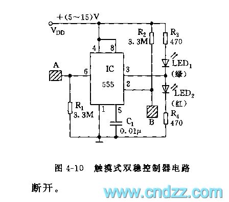
As shown on the figure 4-10, the 555 is the core of this circuit. It uses the 555's 6 foot to contact the comparator A1's in-phase and inverted input of the interior substrate. It can change the output state through controlling the reset and set. When touching the metal disc A, the 555 will be reset, the LED1 will light on and the LED2 will light off. When touching the metal disc B, the LED2 will light on and the LED1 will light off. If changing the relay, we can achieve the control of the executive circuit's power.
(View)
View full Circuit Diagram | Comments | Reading(979)
The rear foglight, defrosting and scraping water theory circuit of 70 road vehicle of Toyota Land Cruiser
Published:2011/6/27 2:48:00 Author:Sophia | Keyword: The rear foglight, defrosting, scraping water theory circuit, 70 road vehicle of Toyota Land Cruiser
Screws commonly used in exterior of lighting to adjust headlamp beam, which is very inconvenient. Japan's Lexus sedan (E5300, Lexus LS400) and the Land Cruiser off-road vehicles all use electronical control to adjust.
Light ball in light bowl have a fairly large space. It uses electromotor to change the place of the light ball (light) in the reflecting mirror to adjust the beam. It can be imagined that the fixing device and Headlamp beam of the bulbs in the interior of lights is more complex.
Figure 1 shows the regulator current from the electromotor of actuating mechanism of fuse F13 (129 relay access from the rear) belongs to the permanent magnet motor, as long as the armature current commutates, the motor rotation will change. Two of relays can be used to change the current direction. When electromotor armature does not work, both ends of the armature phase often combine with electrical contacts. Both ends connecting with the iron can make an effect on dynamic to ensure positioning whiling stopping after adjustment. (View)
View full Circuit Diagram | Comments | Reading(1681)
555 Time-Base Circuit Main Parameters Circuit
Published:2011/7/7 8:19:00 Author:Robert | Keyword: Time-Base, Main, Parameters
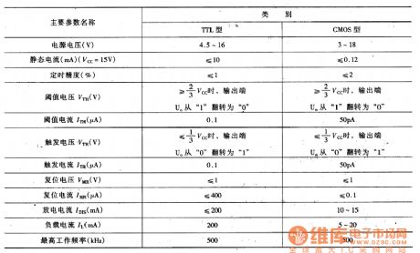
For correctly using the 555 time-base circuit, we should know about its main parameters. The TTL type and CMOS type 555 time-base circuits have difference in their features and parameters. So this table listed their main parameters separately to be used for reference. For dual time-base circuit, the parameters are all the same with the single time-base circuit's except for the its doubling quiescent current. So it can be used by taking the single time-base circuit's main parameters as the reference.
The table shows the 555 time-base circuit's main features and parameters. (View)
View full Circuit Diagram | Comments | Reading(1077)
Work Principle of 555 Monostable Model
Published:2011/7/5 0:01:00 Author:Zoey | Keyword: Work Principle, 555 Monostable Model
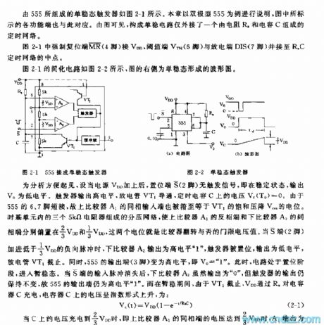
The Monostable multi-vibrator composed of 555 has been shown in the picture 2-1.This chapter takes the bipolar 555 as an example; functional terminals marked in the picture are relevant to each other. This monostable circuit has jointed a time network that consists of a resistance Ra and a capacitor C.
In the picture 2-1, the coercive resetion terminal pin 4 connects VDD, threshold terminal pin 6 VTH and discharge terminal DIS pin7 connect to the midpoint of RaC time network. Picture 2-2 is the simplified circuit, the right one is the waveform of monostable circuit.
When in a stable state, the output voltage V0 is in low level; when the circuit in a temporary stable state, voltage on the capacitor ascends exponentially:
Vc(t)=VDD(1-e-1/RaC)
When voltage on the capacitor reaches to 2/3VDD, the circuit backs to be stable. When the circuit is in a temporary stable state, the time that V0(t) takes to ascend from 0 to 2/3VDD is td:
2/3VDD-VDD(1-e-td/RaC)
From the formulas above, we can conclude that time of outputting high level:
td=-RaCln(1/3)
td≈1.1RaC(s)
The prolonged time of monostable model td is irrelevant to outer voltage VDD but is determined by time constant of time network. (View)
View full Circuit Diagram | Comments | Reading(1037)
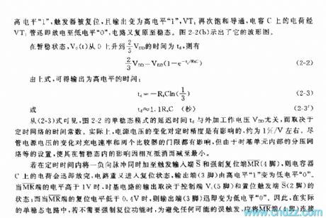
Choice of Circuit Parameter outside 555 Monostable Work Mode
Published:2011/7/5 0:03:00 Author:Zoey | Keyword: Choice, Circuit Parameter, 555 Monostable Work Mode
Basic relationshipbetween monostable model timingand timing network RaC has been shown in picture 2-3.As RaC’s time constant has various mixes, and operation of the circuit is relevant to property of load, trigger level and voltage controlled. Following factors should be taken into consideration to guarantee normal operation of the monostable circuit.
1 Choose a proper value of the time resistance Ra
The minimum value of RaC can be set only if the discharge tube won’t be broken and the maximum value of RaC is determined by threshold current on the comparator A1.
2 Choose a proper value of time capacitance
The minimum value of shall be 100pf or a little bit larger and the maximum value is determined by the leakage current of the capacitor.
3 Driving power
Driving power of 555 is mainly determined by the current property of transistor P6 and Na.
4 Take sensitive loads into consideration
5 Set an accurate time and controllable voltage V
If value of RaC has been set, output pulse width is determined by Vc/VDD. Changing the ratio Vc/VDD to make up the changes arose by capacitance of capacitor, we can set an accurate time.
(View)
View full Circuit Diagram | Comments | Reading(966)
555 Monostable Circuit with a Changeable Width
Published:2011/7/5 0:05:00 Author:Zoey | Keyword: 555 Monostable Circuit with a Changeable Width
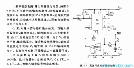
For a general monostable circuit, the pulse width output is a fixed value. As shown in the picture 2-9, pulse in the circuit uses a closed loop to control the manipulative terminal after being magnified, when trigger frequency rises, the temporarily stable pulse width will be narrowed, thus the duty cycle of the wave output remains unchanged.
C2 and R2 trigger the signal input differentially. As the trigger frequency increases, the direct level increases, Vc terminal decreases, and output width of 555 is narrowed. Loop-controlling makes duty cycle output remain unchanged.
Suitable frequency scope for the parameter is 500~5000Hz.When design the circuit, this condition should be guaranteed:R1C1≤1.1Tmin=1.1/fmax,fmax refers to the maximum frequency of trigger signal input. (View)
View full Circuit Diagram | Comments | Reading(1104)
| Pages:21/47 At 202122232425262728293031323334353637383940Under 20 |
Circuit Categories
power supply circuit
Amplifier Circuit
Basic Circuit
LED and Light Circuit
Sensor Circuit
Signal Processing
Electrical Equipment Circuit
Control Circuit
Remote Control Circuit
A/D-D/A Converter Circuit
Audio Circuit
Measuring and Test Circuit
Communication Circuit
Computer-Related Circuit
555 Circuit
Automotive Circuit
Repairing Circuit