
555 Circuit
Index 34
555 belt feeder integrated protector circuit
Published:2011/6/10 20:43:00 Author:nelly | Keyword: belt feeder, integrated protector

Pressing the starting button QA, 12V voltage is added to IC1, IC2, J1 pulls in, the starting ring makes a sound. Once it is added +12V, IC1 is set, when C1 is charged to 2/3 VDD by R1, IC1 is reset. C1's charge time also is the starting delay time td=1.1R1C1, it is about 5s.
T probe in the virtual frame is coal position sensing probe, when the conveyor belt's coal position height touches T probe, it is equal that a no more than 3.2MΩ resistor is between 555's 2 foot and ground , 2 foot's level is lower than 1/3VDD, then IC1 is set, J2 is released, J2-1 is disconnected from the starter, motro M stops running, the electric bell alarms.
(View)
View full Circuit Diagram | Comments | Reading(857)
555 power-limiting circuit with acousto-optic warning alarm function
Published:2011/6/10 21:15:00 Author:nelly | Keyword: power-limiting, acousto-optic warning alarm function
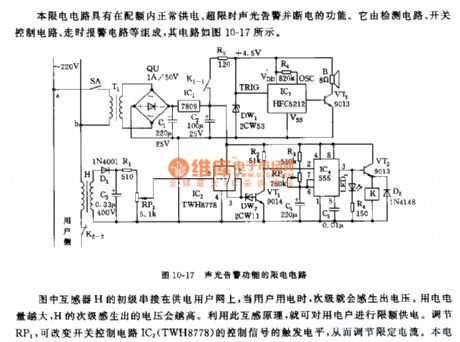
The monostable delay circuit is composed of IC4(555) and R3, RP2, C4. Within power rationing quota, IC2, VT1 all cut off, the 555's set terminal 2 foot is in high level, 555's output terminal 3 foot is low level, relay K is in release condition, its normally closed contact K2-2 is closed, normally open contact K1-1 is shut off. If the user passes beyond the power rationing, the transformer H's secondary voltage increases, IC1 is triggered and conduction, then VT1 is saturation conduction, 555's 2 foot turns to low level, IC4 is set, 3 foot turns to high level, LED1(red)lights, K takes a action(pull in), the user's power supply circuit(K2-2)is cut off, K1-1 closes; IC3 obtains the electricity and triggers, then it emits the warning of dodo, please note .
(View)
View full Circuit Diagram | Comments | Reading(865)
555 simple motor phase failure and overcurrent protection device circuit
Published:2011/6/10 21:45:00 Author:nelly | Keyword: motor phase failure, overcurrent protection device

As shown in the figure 10-21, AC hypotension rectifier circuit provides this circuit with VDD=12V voltage power. The current transformer takes anyone from the three phase motor, after its AC signal is rectificated and filtered, it is used as the monostable delay circuit's comparative voltage which is composed of 555. When it is connected to power supply, 555's 2 foot is low level, 555 is set, 3 foot is high level, J has no action. The short steady time td=1.1(R1+R2)C2, the time constant can be changed by adjusting RC2. When the motor works normally, adjusting RP1, the motor current is turned to lower than 2/3 VDD voltage by LH, it is added to IC's 6 foot.
(View)
View full Circuit Diagram | Comments | Reading(2283)
555 simple electric leakage protector circuit
Published:2011/6/10 22:02:00 Author:nelly | Keyword: electric leakage, protector

As shown in the figure 10-7, the protector is composed of transformer, preamplifier stage and monostable delay circuit and relay. The protection action current is lower than 3mA, the action time is lower than 0.1s.
The transformer HL adopts high conductive magnetic ring, primary fire line and zero line parallel winding 5 turns, secondary polarity winding 500 turns. In normal times, HL's primary line current is in balanced state, secondary polarity does not output signal. When it comes load electric leakage, secondary polarity has signal current, after amplified by VT1, 555's 2 foot is lower than 1/3 VDD, 555 is set, J1 pulls in, J1-2, J1-3 cut off, they are electric leakage protection. VT1 adopts MOSFET, it is voltage control tube, the static work current Ip is about 0.9mA.
(View)
View full Circuit Diagram | Comments | Reading(1199)
555 serial switch regulated power supply circuit
Published:2011/6/10 22:18:00 Author:nelly | Keyword: switch, regulated power supply
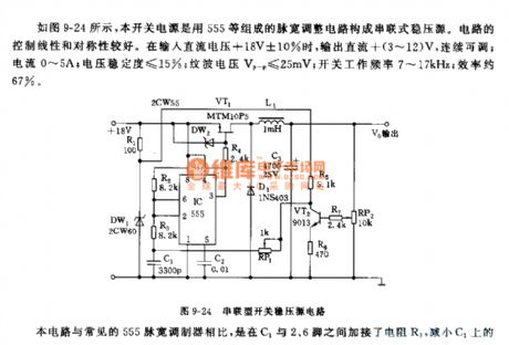
Compared to the usual 555 pulse width modulator, this circuit connects resistance R3 between C1 and 2, 6 feet, it can decrease C1's voltage amplitude. The output voltage sample and amplification circuit are composed of VT2, R5, R6, R7, RP1, RP2, the feedback voltage can be changed by adjusting RP1 and RP2, then the duty ratio of switch square wave and output DC voltage also can be changed. VT1 adopts P groove VMOS tube MTM10P5, the rated current is about 10A. The energy storage induction is about 1mH. D is Fly-wheel diode.
(View)
View full Circuit Diagram | Comments | Reading(1335)
555 hig voltage delay time contact controlled circuit
Published:2011/6/7 1:53:00 Author:nelly | Keyword: high voltage, delay time, contact cotrolled

This circuit is always used in the occasion that the filament need preheat in the vacuum tube equipment. It makes the filament has adequacy time to avoid the cathode added the high pressure under the cold state. As shown on the figure 9-48, the 555 is in the reset mode because the C1's voltage can't mutant. The 555 will reset with the C1 charged when the 2 foot's potential is lower than 1/3VDD. The 3 foot will be the high power level and the J will be pull-in. The contact will contact the high voltage. The delay time, td=1.1RP1C1. The max delay time is about 4 minutes and can use the RP1 to change.
(View)
View full Circuit Diagram | Comments | Reading(953)
555 sectional timing circuit
Published:2011/6/7 1:12:00 Author:nelly | Keyword: sectional, timing
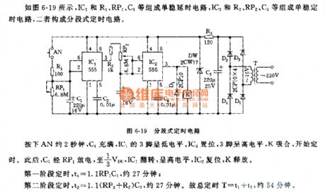
As shown on the figure 6-19, the mono-stable time delay circuit consits of the IC1 and R1,RP1,C1. The mono-stable timing circuit consists of the IC2 and R2,RP2,C3.They constract the sectional timing circuit. Pressing the AN about 2s, the IC1's 3 foot is low power level. The IC2 reset, the 3 foot is high power level and the K will be pull-in. Then the C2 will discharge by the RP1 to the 1/3VDD. The IC1 will flip and be the high power level. The IC2 will reset and K will release. The first timing, t1=1.1RP1C1, about 27 minutes. The second timing, t2=1.1(RP2+R2)C3, about 27 minutes. The total timing, T=t1+t2, about 54 minutes. (View)
View full Circuit Diagram | Comments | Reading(740)
555 novel long timer circuit
Published:2011/6/7 0:56:00 Author:nelly | Keyword: novel, long timer
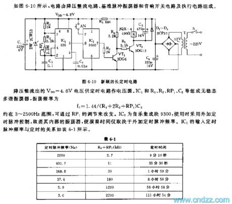
As shown on the figure 6-10, the circuit consists of the hypotension rectifying circuit,reference pulse oscillator, audio switch circuit and executive circuit. The timer circuit's voltage source is 4.8V. The actable multivibrator consists of the IC1 and R1,R2,RP1,C2. The oscillation frequency: f0=1.44/(R1+2R2+RP1)C2. It can be regulated by the RP1. The IC2 is the 9300 music manifold block. It can be controlled by the pulse. Its performance time only depends on the pulse frequency in addition after cancelling its oscillator. The ralations between the IC2's input time pulse frequency and the time are shown on the figure 6-1. (View)
View full Circuit Diagram | Comments | Reading(1085)
555 Sequence timer control circuit
Published:2011/6/7 0:28:00 Author:nelly | Keyword: Sequence, timer control
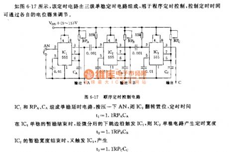
As show on the figure 6-17, this timer circuit consists of the three-level monostable timer circuit. It can be used in the program's timer control and its time can be regulated by thePotentiometer. The monostable delay circuit consists of the IC1 and RPA, CA. Press the AN, the IC1 will filp and reset. The time: t1=1.1RPACA. When the IC1's transient stability is over, the foot edage will trig the IC2, then the IC2 will produce the timer width: t2=1.1RPBCB. The IC2 will trig the IC3 when its transient stability width is over, t3=1.1RPCCC. (View)
View full Circuit Diagram | Comments | Reading(1561)
555 multiple signals generator circuit
Published:2011/6/10 2:27:00 Author:nelly | Keyword: multiple signals, generator
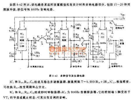
As shown on the figure 8-42, this circuit is the timing and audio circuit parts of the monitoring device model. It includes 15s~20s periodic pulse waveform, second signal and 800Hz audio circuit. The actable multivibrator consists of the IC1 and R16,R19,C12. The oscillation period: T=0.693(R18+2R19)C12. According to the need, we can use the R13 to change the period and the duty ratio. The clock oscillator consists of the IC2 and R23,R24,C13. The IC3 is a 800Hz audio oscillator, its control site's 5 foot is controlled by the VT1's turn-on or cut-off to output variation tone. (View)
View full Circuit Diagram | Comments | Reading(715)
555 pressure sensing digital circuit
Published:2011/6/10 2:00:00 Author:nelly | Keyword: pressure, sensing, digital
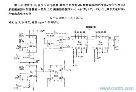
The RX on the figure 8-48 represents the pressure sensor. The Rx changes in proportion with the voltage's change. Taking it as the part of the multivibrator's time constant. The 555 oscillator's frequency: f=1.44/(R1+RX+2R2)C1. Its charge time which means outputing high power level time: t=0.693(R1+R2+RX)C1. we can find the t's big/small is relation to the Rx. (View)
View full Circuit Diagram | Comments | Reading(825)
555 Multi-Wave Generator Circuit (1)
Published:2011/5/19 8:03:00 Author:Robert | Keyword: Multi-Wave, Generator
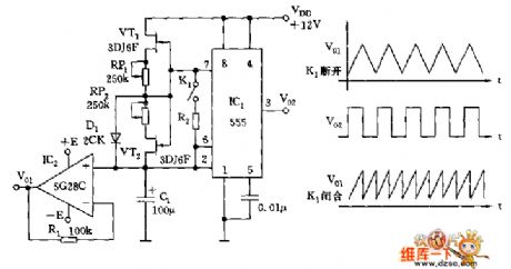
As shown, this circuit is a multivibrator oscillator made up by 555, C1 and constant current charging and discharging circuit. Thc IC2 uses 5G28C as a high-impedance follower device to play the role of isolation and impedance transformation. The oscillator's charging and discharging are all for the constant current source. So its sawtooth wave has a good linearity. RP1 and RP2 are used to adjust the time constant of charging or discharging and the duty ratio separately.
The parameter shown in the picture's cycle time is 0.2ms~60s. When the K1 is disconnected, it would generate sawtooth wave whose cycle is a half of the triangle wave's.
(View)
View full Circuit Diagram | Comments | Reading(2363)
Dodge air-conditioning without transmission circuit
Published:2011/6/8 20:12:00 Author:chopper | Keyword: Dodge, air-conditioning, transmission

View full Circuit Diagram | Comments | Reading(748)
Dodge air-conditioning with transmission control circuit
Published:2011/6/8 7:29:00 Author:chopper | Keyword: Dodge, air-conditioning, transmission control
View full Circuit Diagram | Comments | Reading(735)
Dodge postheating cirucit
Published:2011/6/8 6:49:00 Author:chopper | Keyword: Dodge, postheating

View full Circuit Diagram | Comments | Reading(589)
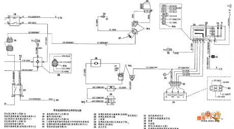
Dodge heater system circuit
Published:2011/6/8 20:08:00 Author:chopper | Keyword: Dodge, heater system
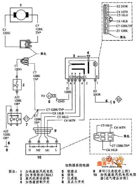
View full Circuit Diagram | Comments | Reading(691)
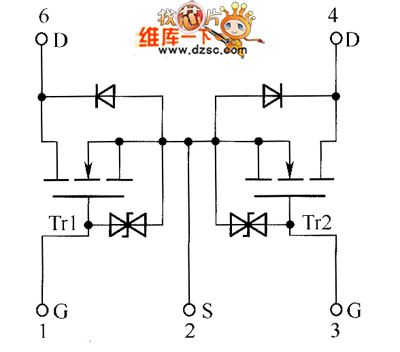
Field-effect transistor US5U1、US5U2、US5U3 internal circuit
Published:2011/6/4 11:38:00 Author:John | Keyword: Field-effect transistor
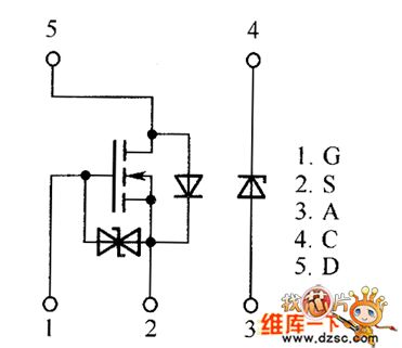
Field-effect transistor US5U1、US5U2、US5U3 internal circuit is shown below.
(View)
View full Circuit Diagram | Comments | Reading(603)
Field-effect transistor UPES120P internal circuit
Published:2011/6/4 11:54:00 Author:John | Keyword: Field-effect transistor
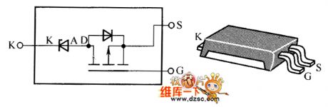
Field-effect transistor UPES120P internal circuit is shown below.
(View)
View full Circuit Diagram | Comments | Reading(668)
Field-effect transistor UM5K1N internal circuit
Published:2011/6/4 12:24:00 Author:John | Keyword: Field-effect transistor
Field-effect transistor UM5K1N internal circuit is shown below.
(View)
View full Circuit Diagram | Comments | Reading(713)
Field-effect transistor STG3P3M25N60 internal circuit
Published:2011/6/4 12:26:00 Author:John | Keyword: Field-effect transistor
Field-effect transistor STG3P3M25N60 internal circuit is shown below.
(View)
View full Circuit Diagram | Comments | Reading(581)
| Pages:34/47 At 202122232425262728293031323334353637383940Under 20 |
Circuit Categories
power supply circuit
Amplifier Circuit
Basic Circuit
LED and Light Circuit
Sensor Circuit
Signal Processing
Electrical Equipment Circuit
Control Circuit
Remote Control Circuit
A/D-D/A Converter Circuit
Audio Circuit
Measuring and Test Circuit
Communication Circuit
Computer-Related Circuit
555 Circuit
Automotive Circuit
Repairing Circuit