
555 Circuit
Index 22
555 Linear Voltage/Frequency Converter Circuit (Three)
Published:2011/7/5 0:07:00 Author:Zoey | Keyword: 555 Linear Voltage, Frequency Converter, Circuit
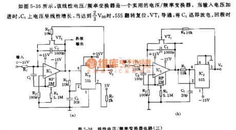
As shown in the picture 5-36, this linear voltage/frequency converter is a practical voltage/frequency converter. When input voltage is strengthened, voltage on C1 will have a linear increase, when it reaches 2/3 VDD, VT1 will conduct and make VT1 discharge promptly. Backhaul time is related to R5C3 time constant. That is,as soon asvoltage on C3 declines to 1/3 VDD, 555 will reset.VT1 will ceases to work, then next timing begins.
Backhaul time of this circuit is only 1μs. The relationship between voltage input and converter frequency can be expressed by following formula:
f=3/2•Vin/VDDR1C1
V/F of parameter in the picture is f ≈10³Vin. If frequency exceeds 10kHz, nonlinear error will be about 0.2%.
(View)
View full Circuit Diagram | Comments | Reading(941)
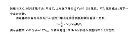
555 Linear Voltage/Frequency Converter circuit (Two)
Published:2011/7/4 23:03:00 Author:Zoey | Keyword: Linear Voltage, Frequency Converter, circuit
As shown in the picture 5-35, this converter is composed of a non-inverting amplifier, an integrator and an oscillator for voltage/frequency conversion.
When jointed to the amplifier, amplification factor K=RF/RA+1 and it is controlled by K1 and K2. IC2, C1, C4 and RP1 constitute a circuit with an active integral, when integral voltage declines to 555 trigger level(<1/3VDD), 555 will set. Meanwhile, VT1 will conduct; integral capacitance will discharge promptly, integral voltage V2 will charge to C2 via R9. When voltage on C2 ascends to 2/3VDD, 555 will reset and give rise to oscillation. Therefore, voltage input is converted to oscillation wave with some frequencies. When input signal ranges from 0 to 2V, frequency of input oscillation varies within the limit from 10Hz to 10 kHz. (View)
View full Circuit Diagram | Comments | Reading(770)
Campbell passive duplex filter circuit
Published:2011/7/4 0:42:00 Author:John | Keyword: passive duplex filter
Campbell's paper gives the author another digital wonders example. That is, the achievement of a functional digital circuit is always superior to the implementation of an analog circuit. He points out that IC filter’s dynamic range depends on the inductance. The bottom of the dynamic range is the thermal noise current (4KTBR) caused by the circuit’s resistance. The top of the dynamic range depends on saturation current of the inductor core. The dynamic range of Campbell’s selected component is up to 180dB. In comparison, the expensive 24-bit audio A / D converter only has 144dB on dynamic range.
(View)
View full Circuit Diagram | Comments | Reading(1053)
SSB modulator based on LM-1496 circuit
Published:2011/7/4 0:29:00 Author:John | Keyword: SSB modulator
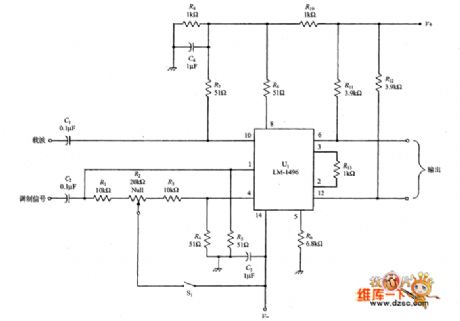
The picture shows the double-sideband suppressed-carrier (DSBSC) signal circuit generated by the LM-1496. When it is followed by connecting the IF-stage with the band-pass filter of the band 2.5 ~ 3kHz, the circuit can also produce single-sideband signal. Usually,carrier signal Vcis generated by a crystal generates and the audio level generates modulated signals Vm through microphone input end or the audio oscillator. J. Carl • Yoshev has ever seen a circuit which is just like a signal generator / test equipment. This circuit can be used for amateur radio and the Navy HF-SSB’s radio transceiver.
(View)
View full Circuit Diagram | Comments | Reading(5390)
Southeast Freeca lighting system circuit
Published:2011/7/4 0:46:00 Author:John | Keyword: lighting system
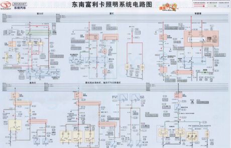
View full Circuit Diagram | Comments | Reading(804)
Audi air conditioning fan circuit
Published:2011/7/4 0:46:00 Author:John | Keyword: air conditioning fan
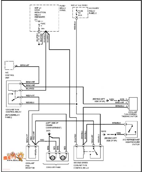
View full Circuit Diagram | Comments | Reading(828)
Four-tier telecommunications filter with ordinary frequency of 1KHZ circuit
Published:2011/7/4 0:44:00 Author:John | Keyword: Four-tier telecommunications filter
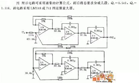
Four-tier telecommunications filter with ordinary frequency of 1KHZ circuit is shown in the following.
The circuit as shown can be applied for the usual formula, and the total requirements will be divided into several paragraphs: Q1 = 0.541, Q2 = 1.306. This circuit uses the LM148 or 741 four-operational amplifiers.
(View)
View full Circuit Diagram | Comments | Reading(721)
Active filter with variable state circuit
Published:2011/7/4 0:44:00 Author:John | Keyword: Active filter
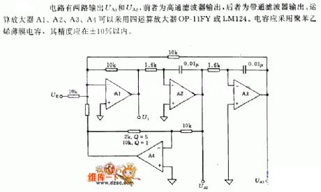
Circuit has two outputs which are named the UA1 and UA2. The former one is called high-pass filter output, and the later one is called band-pass filter output. Four-operational amplifiers four operational amplifiers OP-11FY or LM124 can be used for operational amplifiers A1, A2, A3 and A4. Polystyrene film capacitor can be used and its accuracy should be within ± 10%.
(View)
View full Circuit Diagram | Comments | Reading(778)
Serial communication circuit
Published:2011/7/4 0:30:00 Author:John | Keyword: Serial communication
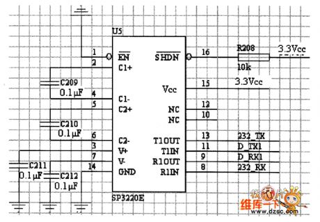
The system implements serial port module is mainly by communicating with the host computer. The microcontroller system will send the collected data to the host computer for processing, thereby reducing the processing burden on the system microcontroller. As electricity level is different when the microcontroller is communicated with the PC interface, interface conversion is needed. The SP3220 chip is used here to complete the conversion on interface’s electricity level. SP3220 chip is with low power consumption and small package and other features. Before the introduction of specific circuits, SP32 ⒛ chip is introduced. SP32 ⒛ chip has the following characteristics.
(View)
View full Circuit Diagram | Comments | Reading(814)
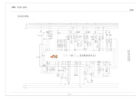
Chery A5/A520 full car circuit
Published:2011/7/6 9:07:00 Author:John | Keyword: full car
View full Circuit Diagram | Comments | Reading(2216)
The Suzuki Antelope-Century Star sensor parameter and engine ABS/SRS system circuit
Published:2011/7/6 1:40:00 Author:qqtang | Keyword: Suzuki, Antelope-Century Star, sensor parameter
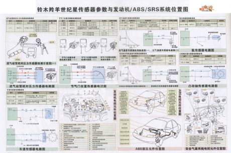
The Suzuki Antelope-Century Star sensor parameter and engine ABS/SRS system circuit is shown as above.
(View)
View full Circuit Diagram | Comments | Reading(1116)
The Toyota A340E“R” back gear oil circuit
Published:2011/6/24 7:41:00 Author:Seven | Keyword: Toyota, back gear
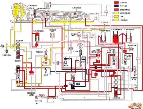
The Toyota A340E“R” back gear oil circuit is shown in the figure.
(View)
View full Circuit Diagram | Comments | Reading(1604)
Mazda 96TAURUS alarm system circuit
Published:2011/7/4 0:42:00 Author:John | Keyword: alarm system
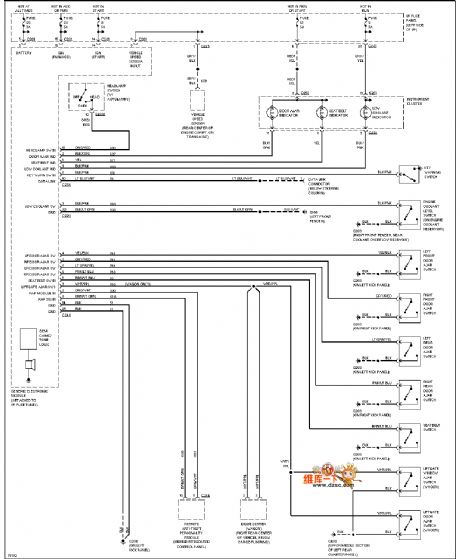
Mazda 96TAURUS alarm system circuit is shown.
(View)
View full Circuit Diagram | Comments | Reading(696)
Mazda 96TAURUS ABS circuit
Published:2011/7/4 0:41:00 Author:John | Keyword: ABS
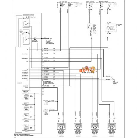
Mazda 96TAURUS ABS circuit is shown.
(View)
View full Circuit Diagram | Comments | Reading(684)
Mazda 96TAURUS power supply circuit
Published:2011/7/4 0:41:00 Author:John | Keyword: power supply
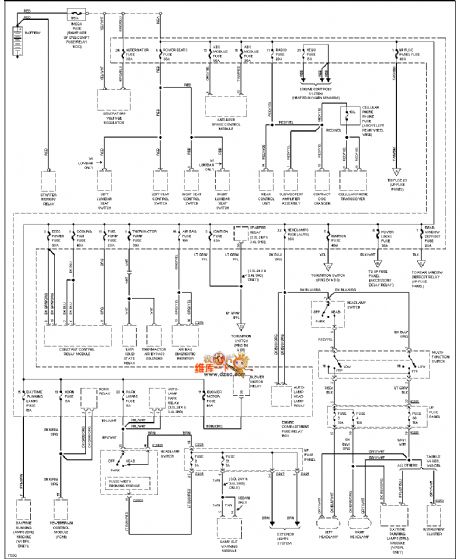
View full Circuit Diagram | Comments | Reading(631)
IF amplifier with a crystal filter circuit
Published:2011/7/4 0:40:00 Author:John | Keyword: IF amplifier, crystal filter
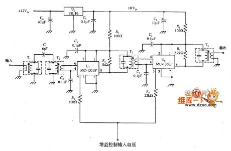
The IF amplifier shown in the figure is based on the design of popular MC-1350P IC. The chip can be gotten by mail from the accessory store or from the smaller stores. This chip is basically the deformation of LM-1490 type and LM-1590 type circuits, but it is easier to use.
If MC-135OP components are not easy to find, the exactly same chip can be found in the online service instead, such as ECG or NTE. These series of components can be bought in the local electronic parts dealers, which are for service and repair shops use. The performance of using MC-1350P chip is identical to that of NTE-746 chip (as well as ECG-746).
(View)
View full Circuit Diagram | Comments | Reading(3458)
555 Audio Oscillator circuit driven by radiofrequency
Published:2011/7/5 0:14:00 Author:Zoey | Keyword: 555 Audio Oscillator circuit, radiofrequency


As shown in the picture 3-14, a 555, R1, RP1,C1 and other parts constitute a controllable audio oscillator, the frequency ofparameter in the picture ranges from 600Hz~20kHz,and it can be selected by adjusting RP1.
Whether the oscillator will oscillate or not is determined by the level on reset terminal of pin 4. Without radio-frequency signal, pin 4 will be in low level and 555 will cease to oscillate; when radiofrequency signal is available, it will be detected by the radiodetector diode D1, and the signal will be sent to pin 4, when the signal level is higher than 1V, the oscillator will oscillate, and the speaker will give out an audio signal that has been adjusted.
Figure 3-14 Audio oscillator circuit driven by radio-frequency Figure3-15 Oscillator circuit in synchronism with clock
(View)
View full Circuit Diagram | Comments | Reading(1266)
11 basic circuits of 555 multi-vibrator
Published:2011/7/5 0:14:00 Author:Zoey | Keyword: 11 basic circuits, 555 multi-vibrator

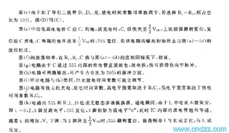
As shown in picture (C), after adding the conduction diode D1 and D2, the charge and discharge time constantwill be separately adjusted. If R1=R2, the duty cycle is 50%. This goes for picture (D), too.
The charge and discharge capacitance arrive at C1 via C, so C1 can get charged to 2/3 VDD quickly and the upper comparator will be turnover and replaced. After being replaced, C will discharge and the voltage of its two terminals will fall to 1/3 VDD, 555 will deposit.
The oscillator frequency in picture (f) is higher than that in (a)~(b);
The circuit in picture (g) can obtain negative narrow pulse;
the circuit in picture(h) can produce a pulse square wave of a 50% duty cycle;
the circuit in picture (i) has an adjustable charge and discharge time constant;
the circuit in picture (j) has independent charge and discharge time constant.
When circuit in picture (k) is galvanized, pin 2and pin 6 will be in high level, 555 will deposit and pin 3 will be in low level of 0, then the discharge tube in IC will be saturated and conducted. f and R will be in direct ratio while f and L will be in inverse ratio. (View)
View full Circuit Diagram | Comments | Reading(1239)
Adjustable Duty cycle 555 Square wave Generator
Published:2011/7/4 22:11:00 Author:Zoey | Keyword: Adjustable, Duty cycle, 555, Square wave Generator
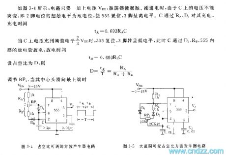
As shown in the figure 3-4, as soon as the voltage VDD is connected, the oscillator starts up. At the beginning of being powered, as the voltage can not be changed suddenly, that is, the starting level of pin 2 is the earth potential, in order to position 555 and leave pin 3 in a state of high level. C charges itself through Ra and D1, the charge time
tc=0.693RaC.
When the voltage on C reaches threshold level, that is 2/3 VDD, pin 3 is in a low level. At that time, C discharges through the discharge tube in D1,Rb and 555. The discharge time
Td=0.693RbC.
Suppose the duty cycle is D, then
D=tc/Td=Ra/Ra+Rb
Adjust RP1, when the center part slide to top,
Dmin=tc/T=1k/1k+11K≈8.3%
When center part of RP1 slide to bottom,
Dmax=11K/11K+1K≈91.7%
Figure3-4 Adjustable Duty cycle Square wave Generator
Figure3-5 Large-scalechangeable Duty cycle Square wave Generator (View)
View full Circuit Diagram | Comments | Reading(1752)
555 Oscillator circuit in synchronism with clock
Published:2011/6/24 2:46:00 Author:Zoey | Keyword: 555Oscillator circuit, in synchronism with clock
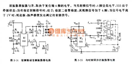

The oscillation of the oscillator is determined by the level of pin 4 in the reset terminal. Without RF signal, pin 4is in low level and 555 ceases to oscillate. When specified RF signal is available, the wave is detected by detector diode D1 and the video signal is placed on pin 4. When signal level turns to be higher than 1V, it starts to oscillate, and the speaker will sent out audio signal adjusted.
Figure3-14 Audio oscillator Circuit driven by RF Figure 3-15 Oscillator circuit in synchronism with clock
As shown in the figure 3-14, 555,R1, RP1 and C1 constitute a controllable audio oscillator, and f=1.44/(R1+2RP1)C1, frequency of parameter in the picture is between 600Hz~20kHz, which can be adjusted by RP1.
(View)
View full Circuit Diagram | Comments | Reading(881)
| Pages:22/47 At 202122232425262728293031323334353637383940Under 20 |
Circuit Categories
power supply circuit
Amplifier Circuit
Basic Circuit
LED and Light Circuit
Sensor Circuit
Signal Processing
Electrical Equipment Circuit
Control Circuit
Remote Control Circuit
A/D-D/A Converter Circuit
Audio Circuit
Measuring and Test Circuit
Communication Circuit
Computer-Related Circuit
555 Circuit
Automotive Circuit
Repairing Circuit