
555 Circuit
Index 12
Operation principle of 555 estable multi-vibrator model
Published:2011/7/30 3:06:00 Author:Zoey | Keyword: 555, Astable Multi-vibrator, Model
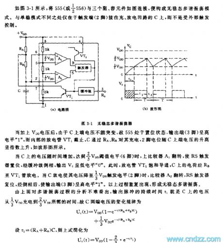
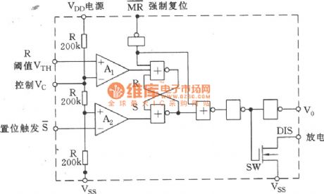
As shown in the picture 3-1, an astable multi-vibrator can be formed after connecting a 555, three resistances and a capacity accessory, the trigger (pin 2) is connected on loop C.
When galvanized voltage VDD, 555 will be reset and pin 3 will havehigh level “1”, the discharge tube VT1 will cease to discharge, and C will get charged via Ra and Rb.
Voltage on C increases along with time, when it gets 2/3 VDD threshold value level, the upper comparator A1 will turn over, RS trigger willset and output a low level”0”, at that time, the discharge tube VT1 will be saturated and conducted, electric charge on C will discharge through Rb to VT1. When C discharges to 1/3 VDD, the upper comparator A2 will turn over, RS trigger willreset and output a high level”1”, this process will be repeated many times.
By analyzing the results, we can conclude that the change rule of voltage on the two terminals of C can be formulated as follow:
Uc(t)=VDD(1-e-t(RA+RB)C)
+1/3 VDDE-t(RA+RB)C
If we replace (RA+RB) with t1, the formula can be simplified as follow:
Uc(t)=VDD(1-2/3•e-t/t1)
Following formula can be concluded:
T=0.693(RA+2RB)C
D=t1/T=(RA+RB)/(RA+2RB)
If RA>>RB, then D≈50%, the output oscillation wave is square wave.
finally we can draw following conclusions:
(1) The oscillation period is not relevant to VDD, but is determined by charge and discharge time constant, that is, the value of RA, RB, and C
(2) Duty cycle of the oscillation is not relevant to C , but is relevant to the ratio of RA and RB
(View)
View full Circuit Diagram | Comments | Reading(1140)
555 Voltage-controlled Oscillator Circuit with its Duty Cycle Controlled by Vc Terminal
Published:2011/8/1 23:41:00 Author:Zoey | Keyword: 555 Voltage-controlled Oscillator Circuit, duty cycle , Vc terminal
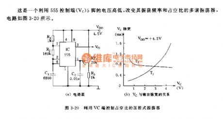
Circuit of the multi-vibratorhas beenshown in thepicture 3-20, oscillator frequency and duty cycle of the vibratorare adjusted according to the level on pin 5, which is controlled by 555 controlling terminal Vc.
A 555, R1, R2 and C1 together constitute an astable multi-vibrator. The controlling terminal can change the level it controlledthrough RP1,it also controls the voltage of comparator A1’s reverse terminal in the chip, adjusts comparator’s baseline voltage so as to change the turnover level of RS trigger and time constant of charge and discharge loop.
As illustrated in picture(b), we can take advantage of the oscillation pulse , which is voltage-controlled, to adjust the voltage of duty cycle without changing oscillation frequency, or to transfer the pulse width, pulse position as well as the voltage. Concrete operation can be seen in 5-26, 5-27 and 5-31,etc in chapter 5.
(View)
View full Circuit Diagram | Comments | Reading(1719)
555 Temperature/Frequency Converter Circuit (two)
Published:2011/8/1 23:39:00 Author:Zoey | Keyword: Temperature, Frequency Converter, circuit
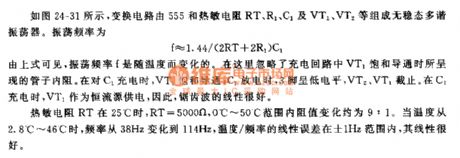
As shown in the picture 24-31, this conversion circuit consists of a 555, and thermosensitive resistances RT, R1, C1, VT1 and VT2, constituting an astable multi-vibrator. The oscillation frequency can be calculated as following formula:
f≈1.44/(2RT+2R1)C1
From the formula above, we can conclude that oscillation frequency varies as temperature change when internal resistance in tube caused by saturation and conduction of charge loop VT1 is neglected. While C1 is charged, VT1 will be saturated and conducted, while C1 is discharging, pin 3 will be in low level and VT2 and VT1 will cease to work. While C1 is charging, VT1 will offer power as a constant current source, therefore,the sawtooh wave will have a good linearity.
If temperature of thermosensitive resistances RT reaches 25℃,RT=5000Ω,variation proportion of internal resistance is about 9:1 when in 0℃~50℃. When temperature ascends to 2.8℃~46℃,frequency will range from 38Hz to 114Hz, liner error of temperare/frequeny will be ±1Hz and linearity will be excellent.
(View)
View full Circuit Diagram | Comments | Reading(1055)
SCHMITT_FROM_555_TIMER
Published:2009/7/2 5:11:00 Author:May
Only three additional parts need be added to standard 555 timer to give fully TTL/DTL-compatible Schmitt trigger that responds to slow input ramps as well as straight DC levels. With output initially high, increasing input from 0 to about 1.35V drives output low. Conversely, input can decrease to about 0.7 V before output goes high again.-M. K. Lalitha and P, R, Chetty, Variable-Threshold Sch mitt Tdgger Uses 555 Timer, EDN Magazine, Sept. 20, 1976, p 112 and 114. (View)
View full Circuit Diagram | Comments | Reading(1125)
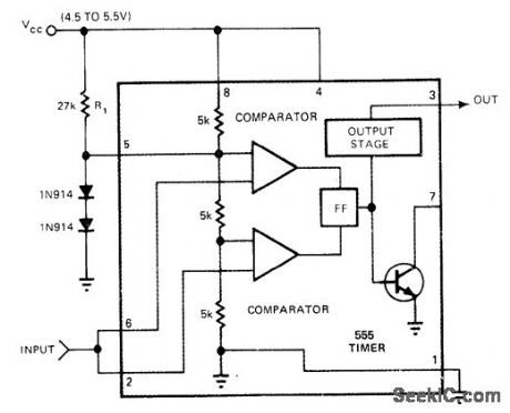
555_TIMER_AS_FLIP_FLOP
Published:2009/7/1 20:21:00 Author:May
Eliminating RC timing network of 555 timer and tying threshold low makes output states depend on trigger and reset inputs. These are pulled high through R1 and R2, then pulled low either with switch or TTL level of 0 on reset input pin 4. Output then stays low until reset goes high and trigger goes low; this bistable action prevents contact bounce from switching output erroneously. Circuit will source or sink 200 mA.-R. L. Gephart, Mini-DIP Bistable Flip-Flop Sinks or Sources 200 mA, EDN Magazine, Oct. 5, 1974, p 76 and 78. (View)
View full Circuit Diagram | Comments | Reading(1458)
SCA_DECODER
Published:2009/7/1 20:17:00 Author:May
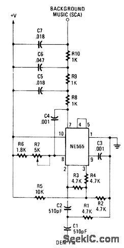
The circuit uses a Signetics NE565 PLL (Phase-Locked Loop) as a detector to recover the SCA signal. The input to the SCA decoder circuit is connected to an FM receiver at a point between the FM discriminator and the de-emphasis filter network. The PLL, IC1, is tuned to 67 kHz by R7, a 5 K potentiometer. Tuning need not be exact since the circuit will seek and lock onto the subcarrier. The demodulated signal from the FM receiver is fed to the input of the 565 through a high-pass filter consisting of two 510 pF capacitors (C1 and C2) and a 4.7 K resistor (R1). Its purpose is to serve as a coupling network and to attenuate some of the main channel spill. The demodulated SCA signal at pin 7 passes through a three-stage de-emphasis network as shown. The resulting signal is around 50 mV, with the response extending to around 7 kHz. (View)
View full Circuit Diagram | Comments | Reading(2793)
NEGATIVE_GOING_DUAL_OUTPUT_555
Published:2009/7/1 20:16:00 Author:May
Circuit triggers on positive-going pulses and delivers negative-going output timing pulses. C1 charges when JFET switch a, is held on by high output state of timer. When output of timer goes low, Ct discharges to ground through Rt. Timing accuracy is good, and duty cycles above 99% are possible without jitter.-W. G. Jung, Take a Fresh Look at New IC Timer Applications, EDN Magazine, March 20, 1977, p 127-135. (View)
View full Circuit Diagram | Comments | Reading(1135)
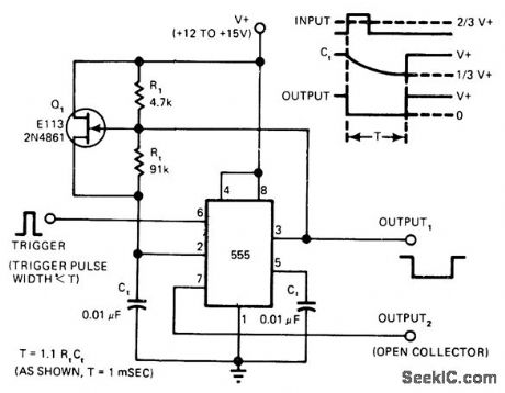
BASIC_555_MONO
Published:2009/7/1 20:06:00 Author:May
Circuit variation shown for original IC timer prototype has same timing equation and input trigger requirements for standard connection but provides two outputs rather than one. This is achieved by using pin 7 of IC as an open-collector output that can be referred to any supply voltage between 0 and +15 V regardless of voltage used for timer. Article describes operation in detail and points out possible drawbacks, including possibility of timing error for high duty cycle operation because C1 takes longer to discharge than in conventional monostable MVBR -W G. Jung, Take a Fresh Look at New IC Timer Applications, EDN Magazine, March 20, 1977, p 127-135. (View)
View full Circuit Diagram | Comments | Reading(944)
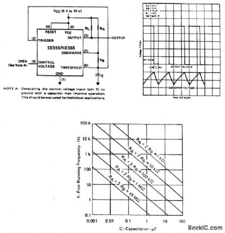
555_ASTABLE
Published:2009/7/1 19:57:00 Author:May
Produces repetitive rectangular output at frequency equal to 1.443/(R1 + 2R2)C hertz. Duty cycle is determined by values of R1 and R2; R2 must be much larger than R1 to obtain nearly a 50% duty cycle. Normal range for duty cycle is S1 to 99%. VCC is 4.5-16 V at 3-10 mA.-H. M. Berlin, IC Timer Review, 73 Magazine, Jan. 1978, p 40-45. (View)
View full Circuit Diagram | Comments | Reading(2724)
using light-emitting diode for piezoelectric signal generator display circuit
Published:2011/7/28 21:47:00 Author:John | Keyword: light-emitting diode, piezoelectric signal generator
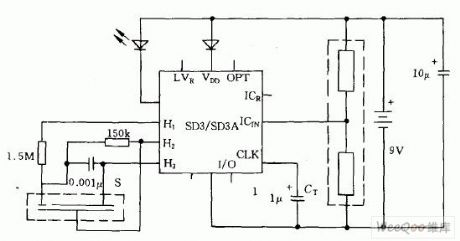
The figure shows the integrated circuit of converting pressure to electrical signal and being sent to SD3 or SD3A followed through the piezoelectric element sensor circuit S. And the signal is displayed through the light-emitting diode. The two equivalent resistors inside of the dashed border of the figure are studio and compensation room respectively (double chamber).
(View)
View full Circuit Diagram | Comments | Reading(1406)
Threshold detector photodiode circuit
Published:2011/7/28 4:28:00 Author:John | Keyword: Threshold detector, photodiode
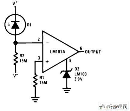
Threshold detector photodiode circuit is shown.
(View)
View full Circuit Diagram | Comments | Reading(3440)
non-inverting summary amplifier circuit
Published:2011/7/28 4:22:00 Author:John | Keyword: non-inverting summary amplifier
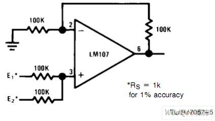
Non-inverting summary amplifier circuit is shown.
(View)
View full Circuit Diagram | Comments | Reading(1043)
Non-inverting amplifier circuit
Published:2011/7/28 4:17:00 Author:John | Keyword: Non-inverting amplifier
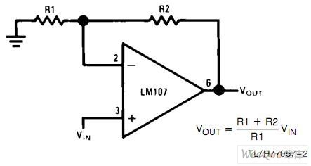
Non-inverting amplifier circuit is shown.
(View)
View full Circuit Diagram | Comments | Reading(1557)
NISSAN new Teana audio (with navigation system) circuit (d)
Published:2011/7/26 4:58:00 Author:John | Keyword: navigation system, new Teana audio
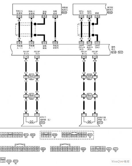
NISSAN new Teana audio (with navigation system) circuit(d)is shown.
(View)
View full Circuit Diagram | Comments | Reading(844)
555 automobile device circuit diagram
Published:2011/7/22 1:22:00 Author:Sophia | Keyword: automobile device circuit
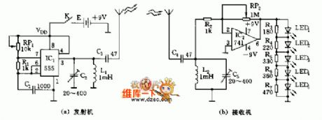
As shown, the car recording device includes the transmitter and receiver. Transmitter constitute oscillator of midband frequency with the core 555, oscillator frequency should be slightly lower than carrier frequency 535KHZ of the AM broadcast, the frequency value depends on R1, RP1, C1, namely f = 1.44 / (RP1 +2 R1). C1, L1, C2 constitute the output resonant circuit, which selects frequency, and then transmit through the C3 by the antenna. Receiving circuit is composed of the input frequency-selective network and 741 op amp. Amplification factor of amplifier depends on RP2/R2. LED1 ~ LED5 is used to indicate received signal strength. Along with the strengthening of the signal, luminotron will be lighted up by the order! !
(View)
View full Circuit Diagram | Comments | Reading(1133)
555 bipolar power conversion circuit
Published:2011/7/21 3:09:00 Author:Ecco | Keyword: 555, bipolar, power conversion
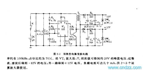
As shown in Figure 9-3, the conversion circuit includes the pulse oscillator and bipolar rectifier circuit. It is used to transfer a group of power supply into two groups of ± 12V DC voltage source in digital circuits and analog mixed circuit board with op amp. The circuit can no longer be set two voltage sources. 555 and R1, R2, C3 form a multivibrator which is in non-steady state, the oscillation frequency f = 1.44 / (R1 +2 R2) C3, the frequency of the icon parameter is about 100kHz, duty cycle is about 70%; the other way gets + 12V voltage. Load current can be up to tens of mA for 2 to 3 op amps.
(View)
View full Circuit Diagram | Comments | Reading(1768)
555 Brightness display circuit
Published:2011/7/21 3:09:00 Author:Ecco | Keyword: 555 , Brightness, display

As shown in Figure 7-32, brightness display circuit includes light sensor, the oscillation circuit and diode display circuit. Photoresistor RG is used as a shunt resistor in 555 oscillator charging loop, with the changing of background light intensity, it shows different resistance, thus affecting the oscillation frequency and the duty cycle of oscillation waveform. When the light intensity increases, the oscillation frequency increases, and the duty cycle reduces, the brightness of light-emitting diode LED increases.
(View)
View full Circuit Diagram | Comments | Reading(1387)
CMOS 555 equivalent function box circuit diagram
Published:2011/7/31 22:08:00 Author:Ecco | Keyword: CMOS, 555 , equivalent function box
View full Circuit Diagram | Comments | Reading(1160)
TTL_MONOSTABLE
Published:2009/6/26 2:04:00 Author:May

View full Circuit Diagram | Comments | Reading(1373)
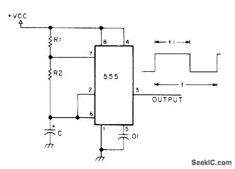
ASTABLE_MULTIVIBRATOR
Published:2009/6/26 1:56:00 Author:May
The capacitor C will charge through RA and RB, and then discharge through RB only.The duty cycle may be controlled by the values of RA and RB. (View)
View full Circuit Diagram | Comments | Reading(0)
| Pages:12/47 1234567891011121314151617181920Under 20 |
Circuit Categories
power supply circuit
Amplifier Circuit
Basic Circuit
LED and Light Circuit
Sensor Circuit
Signal Processing
Electrical Equipment Circuit
Control Circuit
Remote Control Circuit
A/D-D/A Converter Circuit
Audio Circuit
Measuring and Test Circuit
Communication Circuit
Computer-Related Circuit
555 Circuit
Automotive Circuit
Repairing Circuit