
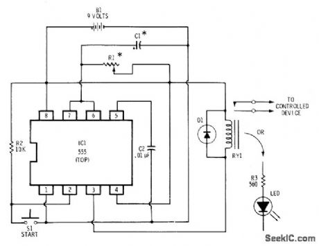
555 Circuit
Index 10
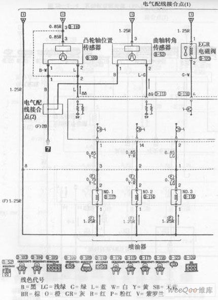
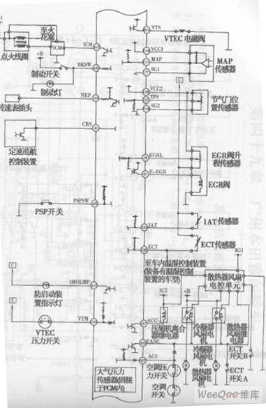
The emission control and air conditioning schematic circuit of Toyota Land Cruiser 70 light-duty off-road vehicle
Published:2011/8/9 19:57:00 Author:Sophia | Keyword: The emission control and air schematic conditioning, Toyota Land Cruiser 70 light-duty off-road vehicle
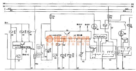
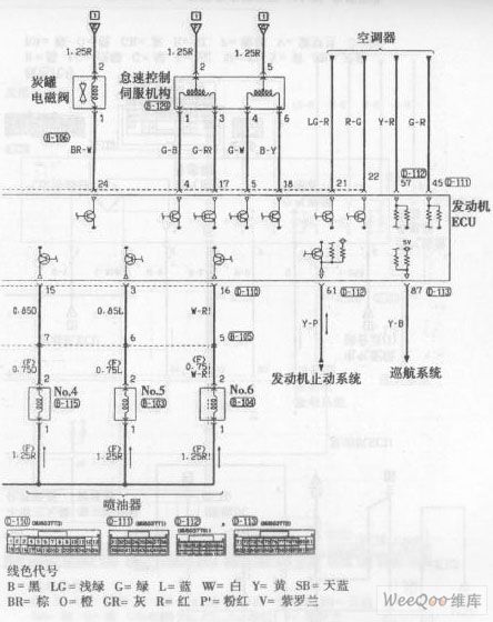
Air conditioning control circuit is mainly to control electromagnetic clutch 52 and the air conditioning blowers 56, 59. Seen from the figure, the blower can be controlled by manpower, and only the blower 56 operating under the premise of air conditioning, compressor 52 are allowed to work.
Air-conditioning amplifier's input signal: A / C thermostat 53, air-conditioning coolant temperature switch 50 (relay 54 is to cut off the circuit of solenoid valve 51, which makes the fast idle speed changed to normal idle speed), dual pressure switch (low voltage lines switches and high-pressure pipeline switch) 48, which can be connected to air-conditioning amplifier control circuit, the supply current flows from F8.)
The Actuating mechanism of air-conditioning amplifier 55 is the compressor magnetic clutch actuator 52 and fast idle solenoid valve. When the current heater motor switch 61 is Connected, if the ambient temperature is above 10 ℃ or domain thermostat temperature is above 5 ℃, and pipeline pressure is normal, then the amplifier connects to the compressor magnetic clutch and air conditioning and refrigeration cycle to make the engine more fuel fast idle. Until the engine temperature rises to a predetermined value, the thermostat switch is closed; the solenoid valve 51 is off, the engine returns to normal idle speed.
(View)
View full Circuit Diagram | Comments | Reading(3729)
Yage Sedan 4-cylinder Engine Control System Circuit (the 2nd)
Published:2011/8/6 8:54:00 Author:Felicity | Keyword: Yage Sedan, 4-cylinder Engine, Control System
View full Circuit Diagram | Comments | Reading(879)
KIA Maxima Sedan Automatic Transmission Circuit (the 1st)
Published:2011/8/1 2:34:00 Author:Felicity | Keyword: KIA Maxima Sedan, Automatic Transmission Circuit, (the 1st)
View full Circuit Diagram | Comments | Reading(936)
Beijing Pajero SUV Engine Control System (M / T) Circuit (the 1st)
Published:2011/8/1 2:53:00 Author:Felicity | Keyword: Beijing Pajero SUV, Engine Control System (M / T)
Wire color code
B=black LG=light green G=green L=blue W=white Y=yellow SB=sky blue BR= brown O=orange GR=gray R=red P=pink V=violet (View)
View full Circuit Diagram | Comments | Reading(884)
Beijing Pajero SUV Engine Control System (M / T) Circuit (the 2nd)
Published:2011/8/1 2:54:00 Author:Felicity | Keyword: Beijing Pajero SUV, Engine Control System (M / T)
Wire color code
B=black LG=light green G=green L=blue W=white Y=yellow SB=sky blue BR= brown O=orange GR=gray R=red P=pink V=violet (View)
View full Circuit Diagram | Comments | Reading(865)
Beijing Pajero SUV Engine Control System (M / T) Circuit (the 3rd)
Published:2011/8/1 2:54:00 Author:Felicity | Keyword: Beijing Pajero SUV, Engine Control System (M / T), (the 3rd)
Wire color code
B=black LG=light green G=green L=blue W=white Y=yellow SB=sky blue BR= brown O=orange GR=gray R=red P=pink V=violet (View)
View full Circuit Diagram | Comments | Reading(835)
Beijing Pajero SUV Engine Control System (M / T) Circuit (the 4th)
Published:2011/8/1 2:43:00 Author:Felicity | Keyword: Beijing Pajero SUV, Engine Control System (M / T), (the 4th)
View full Circuit Diagram | Comments | Reading(840)
Hyundai Sonata Car Cruise Control Circuit (the 1st)
Published:2011/8/1 2:43:00 Author:Felicity | Keyword: Hyundai Sonata Car, Cruise Control
View full Circuit Diagram | Comments | Reading(1207)
555 tri-state acousto-optic logic pen circuit
Published:2011/8/4 8:57:00 Author:nelly | Keyword: tri-state, acousto-optic, logic pen
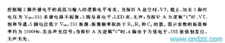
In fact, the 555's control site 5 foot and threshold site 6 foot are the input terminal of the voltage comparator I. If the 6 foot voltage is 5mv larger than the 5 foot's, the 555 will relability trig. Adding the DC voltage to the +/- shown on the figure 7-11. If the voltage is high, the LED1 lights. but if the voltage is low, the LED2 lights. Changing the rangeand RP1. When the two LED lights in turns, the measured voltage equals to multiply the range by the RP1. The measuring range has four planetary: 0-1v,0-10v,0-100v,0-1000v.
(View)
View full Circuit Diagram | Comments | Reading(1540)
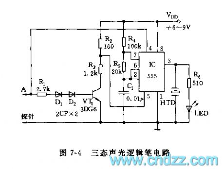
Multi-function integrated security device circuit diagram
Published:2011/8/4 20:00:00 Author:Rebekka | Keyword: Multi-function , integrated security device
Leakage detection circuit is composed of the L1, L2, L3, J1 and so on. The J1 is the leakage detection coil, the relay power from the JZ7-44 isconverted. Under normal circumstances, the current size on the L1, L2 are the same. The phases are contrast. There is no leakage voltage signal in L3. When there is electric shock or leakage occurs, the L3 balance will be destroyed due to the magnetic field induces a voltage signal leakage.
The security devicecan achieve the functions ofleakage protection, overvoltage and undervoltage protection, automatic reset delay (5 minutes or 30 seconds) and so on. (View)
View full Circuit Diagram | Comments | Reading(1410)
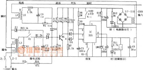
Pulse position modulator (555) circuit
Published:2011/8/6 8:05:00 Author:nelly | Keyword: Pulse position, modulator
(a) circuit diagram (b)waveform (View)
View full Circuit Diagram | Comments | Reading(2355)
Voltage controlled oscillator (555) circuit with the logarithmic characteristic
Published:2011/8/6 2:29:00 Author:nelly | Keyword: voltage controlled, oscillator, logarithmic characteristic
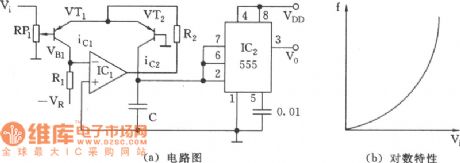
(a) circuit diagram (b)logarithmic characteristic (View)
View full Circuit Diagram | Comments | Reading(1243)
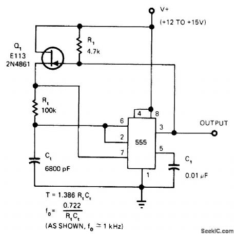
Linear voltage-controlled oscillator (555) circuit
Published:2011/8/6 3:16:00 Author:nelly | Keyword: Linear, voltage-controlled, oscillator
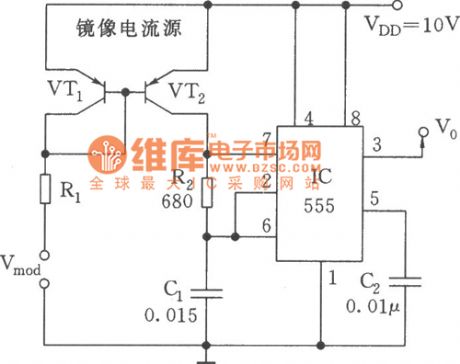
Linear voltage-controlled oscillator (555) circuit is as shown: (View)
View full Circuit Diagram | Comments | Reading(3016)
555_TRIGGER
Published:2009/7/14 22:49:00 Author:Jessie
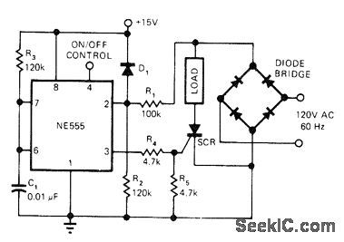
Low-cost 555 timer provides ON/OFF and proportional-control switching of AC loads without generating RFI or voltage spikes. Timer is used in monostable mode, retriggering every half-cycle when voltage at pin 2 falls below about 1.67 V. R3 and C1 fix pulse width at about n ms, long enough to ensure firing SCR in next half-cycle yet short enough to turn SCR off at next zero-crossing without timing-cycle pulse. Pin 4 serves as ON/OFF control input. Varying duty cycle of square wave here gives proportional control for heating and other uses.-M, E, Anglin, Low Cost Zero-Cross Thyristor Trigger Uses a 555 IC, EDN Magazine, Sept. 5, 1977, p 180-181. (View)
View full Circuit Diagram | Comments | Reading(5475)
555_LATCH
Published:2009/7/14 12:10:00 Author:May
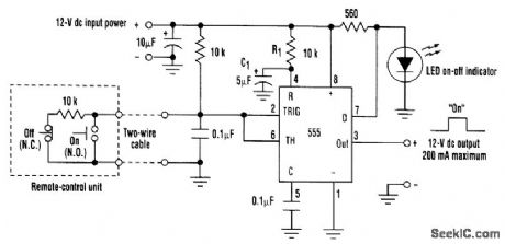
Using a 555 chip in the memory mode, this push-button-cont rolled latch switch can source up to 200 mA of load current. Only one pair of wires is required to interface the ON and OFF push buttons to the control circuitry. The memory-mode feature of the 555 chip is implemented by connecting the trigger (pin 2) and threshold (pin 6) inputs together and applying one-half the supply voltage via a resistor network. Momentarily forcing the input low causes the output to go high, while forcing the input high causes the output to go low. To facilitate remote operation of the latch switch using one pair of wires, one resistor in the voltage-divider network is installed in the remote-control unit. Shorting this resistor out with the ON push button causes the output to go high. Conversely, opening this resistor with the OFF push button induces the output to go low. The R1-C1 network connected to the RESET input (pin 4) forces the latch to come up in the OFF state when power is first applied. The LED on-off indicator is kept off whenever the discharge output (pin 7) is conducting. When the output (pin 3) goes high. (View)
View full Circuit Diagram | Comments | Reading(4505)
50_DUTY_CYCLE_WITH_555
Published:2009/7/15 2:30:00 Author:Jessie
Provides pure square-wave output without sacrificing allowable range of timing resistance. Q1 replaces conventional timing resistor going to V+. Pull-up resistor R1 is required to switch Q1 fully on when it is driven by output of timer.-W. G. Jung, Take a Fresh Look at New IC Timer Applications, EDN Magazine, March 20, 1977, p 127-135. (View)
View full Circuit Diagram | Comments | Reading(1323)
MAGNET_ACTUATED_IGNITION
Published:2009/7/16 3:35:00 Author:Jessie

Distributor contact points are replaced by magnetic pickup that delivers timed pulses to trigger transistor Q1, driver Q2 and output transistor Q3, with latter controlling primary current through ignition coil. Zenet diode D1 clips voltages exceeding voltage rating of Q3.-S.B. Gray, Home and Auto Controls, Electronics, 36:19, p 52-56. (View)
View full Circuit Diagram | Comments | Reading(2975)
BASIC_555_TIMER
Published:2009/7/13 4:17:00 Author:May
Closing switch S1 momentarily applies activating signal to trigger input pin 2 of timer, to start charging of C1. When C1 charges to two-thirds of supply voltage, timer discharges it to complete timing cycle. Duration of charging interval can be varied from several microseconds to over 5 min by changing values of R1 and C1. With 1K for R1, capacitor values of 0.01 to 100 μF give time range of 10μs to 100 ms. With 100 megohmsand lμF,time increases to 10s. Once timer starts, closing S1 again has no effect. Timing cycle can be interrupted only by applying reset pulse to pin 4 or opening power supply. Circuit will drive LED directly or can be used with miniature relay (Radio Shack 275-004) to control larger loads. Can be used as darkroom timer if LED is kept several feet away from photographic paper. Diode is 1N914.-F.M, Mims, Integrated Circuit Projects, Vol. 2, Radio Shack, Fort Worth, TX, 1977, 2nd Ed., p 57-65. (View)
View full Circuit Diagram | Comments | Reading(1462)
LONG_DELAY_555_MONO
Published:2009/7/13 2:04:00 Author:May

FET-input 3140 opamp is used to multiply effective values of timing components Rt and Ct, eliminating need for high-value precision resistor and large low-leakage capadtor. Combination performs as standard 555 mono except that timing equation is T = 100RtCt (for condition wherein division resistors R1 and R2 are chosen for 91-to-1 operation). Circuit has uncommitted open-collector output from pin 7 of 555, which can be referred to any voltage from 0 to + 15 V. Pin 4 is between pins 6 and 8 on 555.-W. G. Jung, Take a Fresh Look at New IC Timer Applications, EDN Magazine, March 20 1977, p 127-135. (View)
View full Circuit Diagram | Comments | Reading(1455)
Yage Sedan V6 Engine Electronic Control System Circuit (the 2nd)
Published:2011/7/18 2:59:00 Author:Felicity | Keyword: Yage Sedan V6 Engine Electronic Control System Circuit (the 2nd)
View full Circuit Diagram | Comments | Reading(910)
| Pages:10/47 1234567891011121314151617181920Under 20 |
Circuit Categories
power supply circuit
Amplifier Circuit
Basic Circuit
LED and Light Circuit
Sensor Circuit
Signal Processing
Electrical Equipment Circuit
Control Circuit
Remote Control Circuit
A/D-D/A Converter Circuit
Audio Circuit
Measuring and Test Circuit
Communication Circuit
Computer-Related Circuit
555 Circuit
Automotive Circuit
Repairing Circuit