
Index 224
High voltage high exchange rate power amplifier circuit diagram
Published:2011/5/11 4:08:00 Author:Rebekka | Keyword: High voltage , high exchange rate, power amplifier
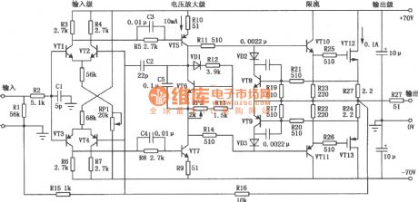
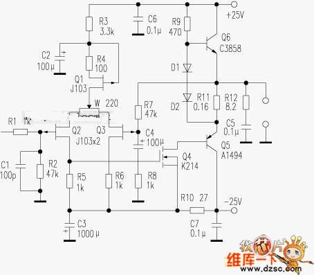
High voltage high exchange rate power amplifier circuit composed of MOSFET is shown as above.
Output stage uses power MOSFET tube. It can improve the frequency characteristics and play a protective role when it is abnormal loads. The circuit is comosed of input stage, voltage amplifier stage, current limit level and the output stage 4 parts. (View)
View full Circuit Diagram | Comments | Reading(7490)
The recording and playing circuit composed of SLA4100
Published:2011/5/11 3:21:00 Author:Rebekka | Keyword: recording and sending out
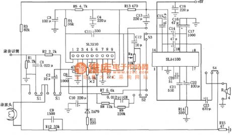
The features of SLA4100 audio power integrated amplifier are: Power supply voltage is low, the adaptability of power falling is strong, low noise, high fidelity characteristics etc. It is suitable for FM, AM radio cassette recorders, record players and power amplifier. The recording and playing circuit composed of SLA4100 is shown as above. (View)
View full Circuit Diagram | Comments | Reading(652)
High-gain amplifier circuit composed of CW117 CW217 CW317
Published:2011/5/11 3:39:00 Author:Rebekka | Keyword: High-gain amplifier
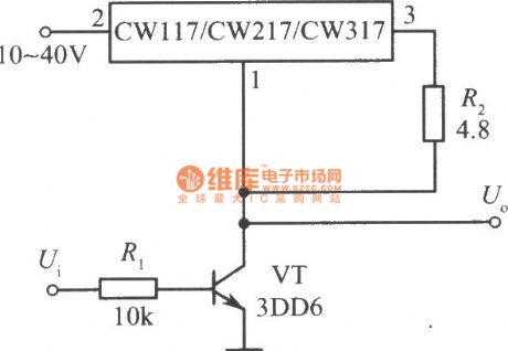
High-gain amplifier circuit composed of CW117, CW217 andCW317 is shown as above. (View)
View full Circuit Diagram | Comments | Reading(674)
Basic in-phase amplified circuit diagram composed of μA709
Published:2011/5/11 4:18:00 Author:Rebekka | Keyword: Basic in-phase amplified
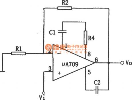
Basic relations:
R1-The input resistance operational amplifierR2-The output resistance operational amplifierRV-Operational amplifier open-loop amplification
Basic in-phase amplified circuit diagram composed of μA709 is shown as above.
(View)
View full Circuit Diagram | Comments | Reading(617)
Portable digital amplifier PWM D type amplification circuit diagram
Published:2011/5/11 4:40:00 Author:Rebekka | Keyword: Portable digital amplifier , PWM D type amplification

Portable digital amplifier PWM D type amplification circuit diagram is shown as above. (View)
View full Circuit Diagram | Comments | Reading(3305)
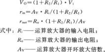
Power amplifier circuit composed of HIP4080A
Published:2011/5/11 3:03:00 Author:Rebekka | Keyword: power amplifier
Power amplifier circuit composed of HIP4080A is shown as above. (View)
View full Circuit Diagram | Comments | Reading(2882)
C22 power amplifier circuit diagram
Published:2011/5/11 3:25:00 Author:Nicole | Keyword: power amplifier
View full Circuit Diagram | Comments | Reading(915)
30W category A power amplifier circuit diagram
Published:2011/5/11 3:24:00 Author:Nicole | Keyword: 30W power amplifier, category A
View full Circuit Diagram | Comments | Reading(1122)
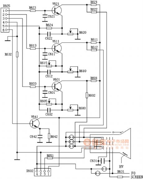
TDA6108 TV video amplifier circuit diagram
Published:2011/5/11 2:25:00 Author:Ecco | Keyword: TV video , amplifier
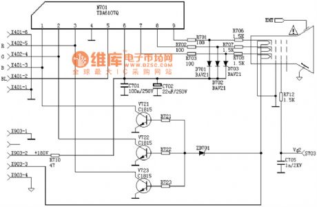
TDA6108 TV video amplifier circuit diagram
(View)
View full Circuit Diagram | Comments | Reading(3523)
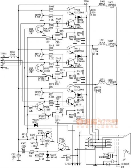
TV video amplifier circuit diagram 6
Published:2011/5/11 1:56:00 Author:Ecco | Keyword: TV video , amplifier
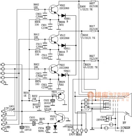
TV video amplifier circuit diagram 6
(View)
View full Circuit Diagram | Comments | Reading(891)
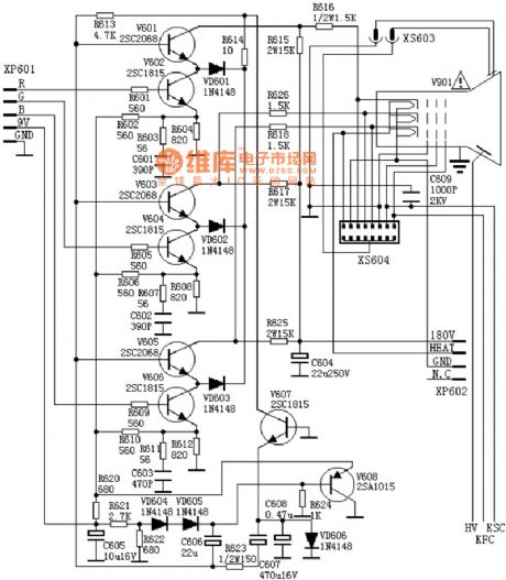
TV video amplifier circuit diagram 5
Published:2011/5/11 1:58:00 Author:Ecco | Keyword: TV video , amplifier
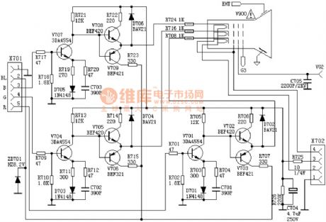
TV video amplifier circuit diagram 5
(View)
View full Circuit Diagram | Comments | Reading(1757)
TV video amplifier circuit diagram 4
Published:2011/5/11 1:59:00 Author:Ecco | Keyword: TV video , amplifier
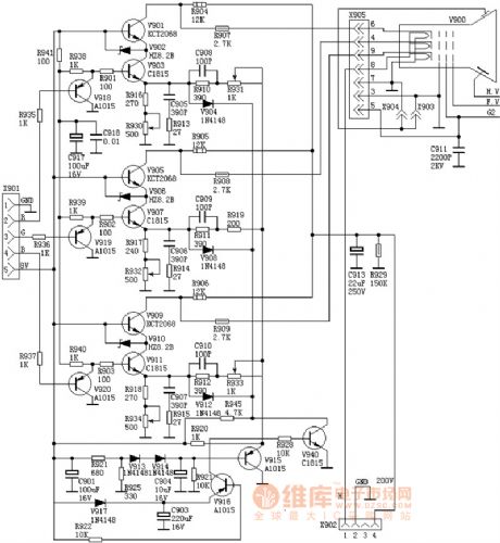
TV video amplifier circuit diagram 4
(View)
View full Circuit Diagram | Comments | Reading(610)
TV video amplifier circuit diagram 3
Published:2011/5/11 1:54:00 Author:Ecco | Keyword: TV video , amplifier
TV video amplifier circuit diagram 3
(View)
View full Circuit Diagram | Comments | Reading(1151)
TV video amplifier circuit diagram 2
Published:2011/5/11 1:55:00 Author:Ecco | Keyword: TV video , amplifier
TV video amplifier circuit diagram 2
(View)
View full Circuit Diagram | Comments | Reading(1197)
TV video amplifier circuit diagram 1
Published:2011/5/11 1:56:00 Author:Ecco | Keyword: TV video , amplifier
TV video amplifier circuit diagram 1
(View)
View full Circuit Diagram | Comments | Reading(812)
Low noise good precision magnetic head amplifier (AD797) circuit
Published:2011/5/10 2:23:00 Author:TaoXi | Keyword: Low noise, good precision, magnetic head amplifier
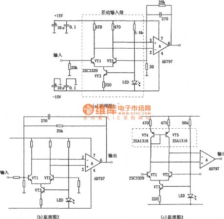

The low noise good precision magnetic head amplifier (AD797) circuit is as shown. These three circuits have different input modes. In figure (a), the input signal with the single-ended input mode adds to the current source-type differential amplifier circuit which is composed of the transistors, and this circuit outputs the signal with differential amplifier mode to the op amp AD797's two input ports (pins 2,3). This circuit uses the differential amplifier which is composed of the transistor structure with excellent performance, so this circuit has high signal to noise ratio (S/N) and can process the signal with larger dynamic range. In figure (a), the three transistors are 2SC3329, VT3 is the constant current tube, VT1 and VT2 are the differential amplification tube. Add the 20kΩ feedback resistor and the 270pF compensation capacitor between the op amp AD797's output port (pin 6) and VT2's base pin. Feedback resistor of the 20Ω resistance from VT2 to ground and the 20kΩ feedback resistor decide the voltage gain, the 270pF compensation capacitor improves the stability of the circuit. You need to add two resistances (10μF electrolytic capacitor and 0.1μF organic synthetic membranes capacitance) between the positive and negative power supply terminals (pin 7,4) and the ground as the decoupling capacitor. You can filter the high-frequency interference and the low-frequency interference in this way.
(View)
View full Circuit Diagram | Comments | Reading(2649)
CDO031AM-16bitD/A converter integrated circuit
Published:2011/5/10 1:00:00 Author: | Keyword: converter

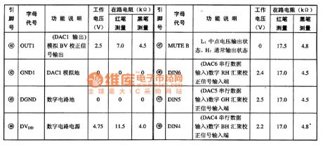
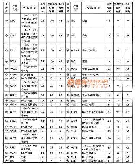

CDO031AM is a 16bitD / A converter integrated circuit.It's used widely in changhong remarkable series of fine,the rear movement color TV.
1. Features
CDO031AM integrated circuit's interior is mainly composed of digital convergence correction circuit RV,digital convergence correction circuit GV,digital convergence correction circuit BV,analog BH correction circuit,analog RH correction circuit,analog GH correction circuit,clock circuit,reference voltage circuit, DAC circuit, DAC Central power supply circuit, the digital power supply circuit, analog power circuits and other features supporting circuit.
2. pin functions and data
CDO031AM integrated circuit uses 48-pin DIP package structure.The pin function and data are listed in table 1.
Table 1 CDO031AM integrated circuit's pin function and data
Tip: CDO031AM integrated circuit has more supply pins, different circuit supply the power introduced by different pin,.when repairing the circuit,we should test the corresponding power supply pins. (View)
View full Circuit Diagram | Comments | Reading(548)
TA869OAN, TA869lAN single chip dual-mode color TV circuit
Published:2011/5/10 2:25:00 Author:TaoXi | Keyword: single chip, dual-mode, color TV
The TA869OAN and TA869lAN are designed as the single chip dual-mode color TV circuit that is produced by the TOSHIBA company, and they can be used in the domestic and imported color TVs.
1.Features
The TA869OAN and TA869lAN has the image IF function circuit, the sound IF function circuit, the video function circuit, the color function circuit and the line field small signal circuit.
2.Pin functions and data
The difference between TA869OAN and TA869lAN is the reverse and positive of the RF AGC control, the manifold in-circuit block diagram, the pin functions and data is as shown in figure 1.
Table 1 The pin functions and data of the TA872OAN (View)
View full Circuit Diagram | Comments | Reading(836)
CAT24C16F electric erasable and programmable read only memory integrated circuit diagram
Published:2011/5/10 1:16:00 Author:Fiona | Keyword: electric erasable, programmable read only memory
(View)
View full Circuit Diagram | Comments | Reading(535)
High-voltage Linear SCR Amplification Circuit
Published:2011/5/10 4:21:00 Author:Sharon | Keyword: High-voltage, Linear, SCR, Amplification
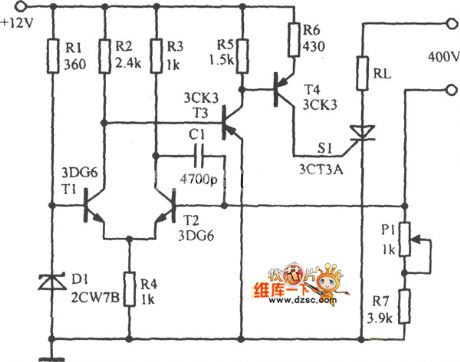
High-voltage Linear SCR Amplification Circuit is shown in below figure:
(View)
View full Circuit Diagram | Comments | Reading(866)
| Pages:224/250 At 20221222223224225226227228229230231232233234235236237238239240Under 20 |
Circuit Categories
power supply circuit
Amplifier Circuit
Basic Circuit
LED and Light Circuit
Sensor Circuit
Signal Processing
Electrical Equipment Circuit
Control Circuit
Remote Control Circuit
A/D-D/A Converter Circuit
Audio Circuit
Measuring and Test Circuit
Communication Circuit
Computer-Related Circuit
555 Circuit
Automotive Circuit
Repairing Circuit