
Index 235
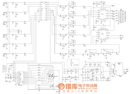
Ultrashort wave antenna amplifier circuit
Published:2011/5/2 9:06:00 Author:Christina | Keyword: Ultrashort wave, antenna, amplifier

The Ultrashort wave antenna amplifier circuit is as shown:
(View)
View full Circuit Diagram | Comments | Reading(680)
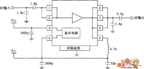
RF2320 linear general amplifier pin circuit
Published:2011/5/2 2:25:00 Author:Christina | Keyword: linear, general amplifier, pin circuit
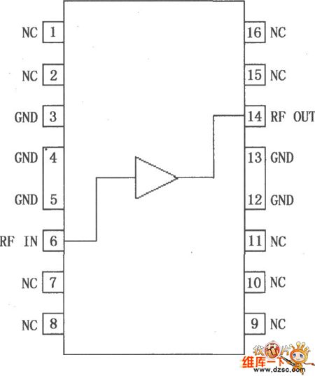
The RF2320 is one kind of general-purpose, low-cost, high-efficiency linear RF amplifier IC, this device has the GaAs heterojunction bipolar transistor (HBT) treatment, and it is designed for the cascade 75Ω gain circuit (Value of noise is less than 2dB), in the range of 5~1000 MHz, the gain flatness is better than 0.5dB, high linearity makes this device can be used in the cable and TV applications. Also the RF2320 can be used in wireless voice and data communications products' IF and RF amplification, the band up to 2500MHz, the device itself contains the 75Ω, the input impedance and output impedance and it supplies the 2:1 VSWR (Voltage Standing Wave Ratio). The RF2320 CATV can be used in distribution amplifier, cable modem, broadband gain blocks, laser diode driver, reciprocating-channel amplifier, base station applications. And the RF2320 is in the square bat-winged SOP-16 package, the pin out is as shown in figure.
(View)
View full Circuit Diagram | Comments | Reading(744)
Transistor storage time test circuit
Published:2011/5/2 5:36:00 Author:Christina | Keyword: Transistor, storage time, test circuit
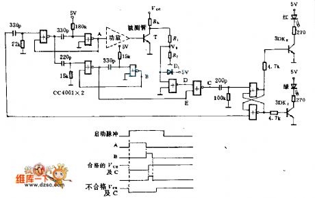
This circuit uses two pieces of CMOSCC4001. If the measure time and the storage time of T is less than the maximum allowable value, the green light turns on, this means qualified; the TS is too large, so the red light turns on, this means unqualified.
Add the pulse to begin testing, point A's pulse width is about 50μS, during the test tube T conducted. Point B's pulse width is about 4μS, this is the T's maximum allowable storage time. If TS<4μS, the C will be 1 , RS flip-flop does not turn, so the red light turns on, green turns off.
(View)
View full Circuit Diagram | Comments | Reading(860)
Cathode output amp tube circuit
Published:2011/5/2 9:17:00 Author:Christina | Keyword: Cathode output, amp tube
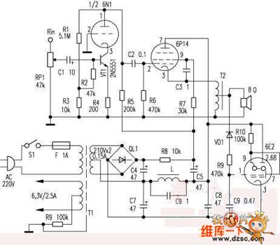
Features of this circuit are the cathode output and the autotransformer, the voltage amplifier stage is very special. This circuit intended to improve the control of amp tube, and to improve the sound clarity.
(View)
View full Circuit Diagram | Comments | Reading(973)
Suzuki GSX400F motorcycle decomposition circuit
Published:2011/5/2 18:41:00 Author:Christina | Keyword: Suzuki, motorcycle, decomposition
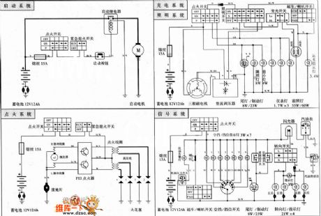
The Suzuki GSX400F motorcycle decomposition circuit is as shown:
(View)
View full Circuit Diagram | Comments | Reading(2250)
CNC lathe test circuit
Published:2011/5/2 19:19:00 Author:Christina | Keyword: CNC, lathe test
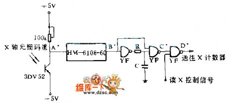
This circuit converts the X-axis's (or Y axis) rotation angle into the optical pulse, and then the photodiode 3DU52 converts the optical signal into electric signal, and outputs the pulse by GD plastic RC circuit to the counter, to achieve closed-loop control system.
(View)
View full Circuit Diagram | Comments | Reading(796)
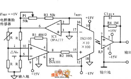
Driver Circuit of Bridge Sensor
Published:2011/5/2 2:25:00 Author:Felicity | Keyword: Driver Circuit of Bridge Sensor,
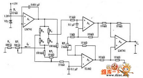
The picture shows the driver circuit of bridge sensor. We can see that in this circuit A1 is the constant current output circuit where the constent value is determined by UZ(the steady voltage of VD1) and (R(RP1)+R2). It provides the patialvalue ofconstant currentto the bridge sensor(the bridge circuit consisting of RA-RD). The amplifier which consisting of A2-A4 can magnify the signals which was outputed by seneors to the level needed. (View)
View full Circuit Diagram | Comments | Reading(665)
Current Control Circuit of Differential Amplifier
Published:2011/5/2 2:38:00 Author:Felicity | Keyword: Current Control Circuit of Differential Amplifier,

View full Circuit Diagram | Comments | Reading(631)
Video amplification circuit composed of discrete device
Published:2011/4/29 4:29:00 Author:Rebekka | Keyword: discrete device, Video amplification
Video amplification circuit composed of discrete device. (View)
View full Circuit Diagram | Comments | Reading(705)
Voice switch input amplification circuit diagram
Published:2011/4/29 1:27:00 Author:Rebekka | Keyword: Voice Switch, input amplification

Voice switch input amplification circuit diagram is shown as above. (View)
View full Circuit Diagram | Comments | Reading(624)
RS232 serial port to RS485 conversion interface circuit diagram
Published:2011/4/29 3:12:00 Author:Rebekka | Keyword: conversion interface
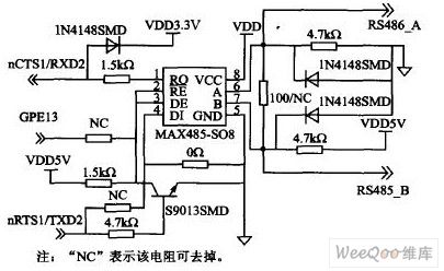
RS232 to RS485 conversion interface circuit diagram designed by MAX485 chip is shown as above. (View)
View full Circuit Diagram | Comments | Reading(3321)
Portable DTMF electronics dialer circuit diagram
Published:2011/4/29 3:09:00 Author:Rebekka | Keyword: Portable DTMF , electronics dialer
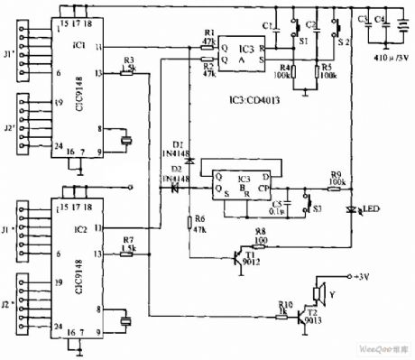
DTMF dialer portable electronic circuit is shown as above. The portable electronic DTMF dialer circuit is composed of the two private number plate C1C9148 and other digital circuit. The electronic dialer mainly use two disc special circuit CIC9148, each plate number unit can store 19 phone numbers that one number has 16 numbers. Two circuits can store 38 numbers. (View)
View full Circuit Diagram | Comments | Reading(1323)
TA7550S audio amplifier integrated circuit
Published:2011/4/29 1:30:00 Author:TaoXi | Keyword: audio amplifier

The TA75550S is designed as one kind of audio amplifier integrated circuit which is produced by the TOSHIBA company, and it can be used in large screen and rear projection TV such as the Konka BT5O01 rear projection TV.etc.
1.Features
The TA75550S has two-stage amplifier with the same functions. The two-stage op amp only supplies power to TA75550S, so the distortion is very small.
2.Pin functions and data
The TA75550S is in the 9-pin single in-line package, and the pin functions and data is as shown in table 1.
Table 1 The pin functions and data of TA75550S (View)
View full Circuit Diagram | Comments | Reading(743)
Logarithmic amplification circuit
Published:2011/4/2 4:06:00 Author:may | Keyword: Logarithmic amplification
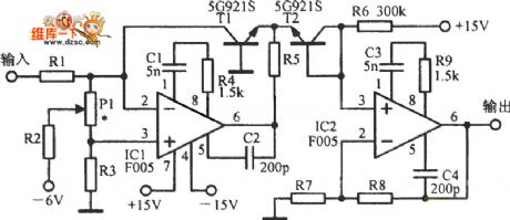
Logarithmic amplification is show in the following picture:
(View)
View full Circuit Diagram | Comments | Reading(679)
Practical high speed logarithmic amplifier circuit
Published:2011/4/23 1:04:00 Author:May | Keyword: logarithmic amplifier
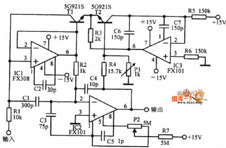
Practical high speed logarithmic amplifier circuit is shown in the following picture:
(View)
View full Circuit Diagram | Comments | Reading(879)
Logarithmic amplifier with temperature compensation circuit
Published:2011/4/23 1:04:00 Author:May | Keyword: logarithmic amplifier, temperature compensation
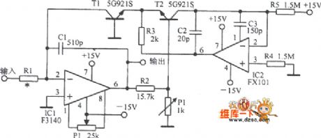
Logarithmic amplifier with temperature compensation circuit is shown in the following picture:
(View)
View full Circuit Diagram | Comments | Reading(2587)
5.1-channel amplifier system circuit diagram
Published:2011/4/29 0:51:00 Author:Ecco | Keyword: 5.1-channel, amplifier system
View full Circuit Diagram | Comments | Reading(10261)
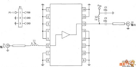
2450MHz final level high power linear amplifier circuit composed of RF2126
Published:2011/4/23 2:22:00 Author:May | Keyword: 2450MHz, final level, high power, linear amplifier
The picture is 2450MHz final level high power linear amplifier circuit composed of RF2126. Radio-frequency signal (RF) inputs by pin 1, and enlarge by power amplifier then output by pin 7 ( 5, 6, 8) . Pin 1 direct coupling with inside amplifier, so add a blocking coupling capacitance out of it. capacity of blocking coupling capacitance is 1.8~2.0μF, input resistance of pin 1 is 50Ω. The capacitance and inductance in the picture is the typical value when frequency is 2450MHz.
(View)
View full Circuit Diagram | Comments | Reading(1457)
Bridge isolated amplifier circuit
Published:2011/4/6 5:37:00 Author:may | Keyword: Bridge isolated amplifier
Bridge isolated amplifier circuitis shown in the following diagram:
(View)
View full Circuit Diagram | Comments | Reading(648)
50Ω impedance linear amplifier circuit composed of the RF2320
Published:2011/4/28 19:14:00 Author:Christina | Keyword: 50Ω, impedance linear amplifier
The 50Ω impedance linear amplifier circuit composed of the RF2320 is as shown:
(View)
View full Circuit Diagram | Comments | Reading(507)
| Pages:235/250 At 20221222223224225226227228229230231232233234235236237238239240Under 20 |
Circuit Categories
power supply circuit
Amplifier Circuit
Basic Circuit
LED and Light Circuit
Sensor Circuit
Signal Processing
Electrical Equipment Circuit
Control Circuit
Remote Control Circuit
A/D-D/A Converter Circuit
Audio Circuit
Measuring and Test Circuit
Communication Circuit
Computer-Related Circuit
555 Circuit
Automotive Circuit
Repairing Circuit