
Index 234
H7N0308LS Internal Circuit
Published:2011/5/3 9:10:00 Author:Felicity | Keyword: Internal Circuit

The picture above shows the H7N0308LS Internal Circuit. (View)
View full Circuit Diagram | Comments | Reading(449)
H7N0203AB Internal Circuit
Published:2011/5/3 9:21:00 Author:Felicity | Keyword: Internal Circuit

The picture above shows the H7N0203AB Internal Circuit. (View)
View full Circuit Diagram | Comments | Reading(460)
H7N0308AB Internal Circuit
Published:2011/5/3 9:14:00 Author:Felicity | Keyword: Internal Circuit

The picture above shows the H7N0308AB Internal Circuit. (View)
View full Circuit Diagram | Comments | Reading(450)
H7N0308LD Internal Circuit
Published:2011/5/3 9:12:00 Author:Felicity | Keyword: Internal Circuit

The picture above shows the H7N0308LD Internal Circuit. (View)
View full Circuit Diagram | Comments | Reading(407)
H7N0307LS Internal Circuit
Published:2011/5/3 9:17:00 Author:Felicity | Keyword: Internal Circuit
The picture above shows the H7N0307LS Internal Circuit. (View)
View full Circuit Diagram | Comments | Reading(566)
H7N0307AB Internal Circuit
Published:2011/5/3 9:20:00 Author:Felicity | Keyword: Internal Circuit,

The picture above shows the H7N0307AB Internal Circuit. (View)
View full Circuit Diagram | Comments | Reading(454)
H7N0307LD Internal Circuit
Published:2011/5/3 9:19:00 Author:Felicity | Keyword: Internal Circuit

The picture above shows the H7N0307LD Internal Circuit. (View)
View full Circuit Diagram | Comments | Reading(435)
Bridge sensor signal amplifier AD22055 typical application circuit diagram
Published:2011/5/3 3:17:00 Author:Rebekka | Keyword: Bridge sensor signal amplifier, typical application circuit
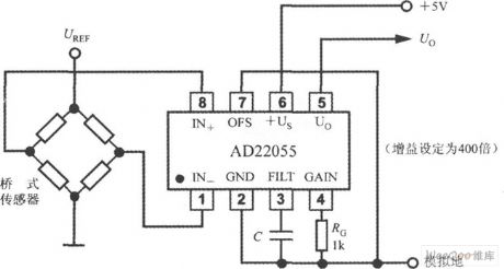
Bridge sensor signal amplifier AD22055 typical application circuit diagram. (View)
View full Circuit Diagram | Comments | Reading(917)
1W superhigh frequency power amplifier circuit
Published:2011/3/23 4:49:00 Author:may | Keyword: superhigh frequency power amplifier
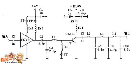
1W superhigh frequency power amplifier circuit is shown in the following diagram:
(View)
View full Circuit Diagram | Comments | Reading(760)
NTA4153N、NET4153N Internal Circuit
Published:2011/5/3 2:59:00 Author:Felicity | Keyword: Internal Circuit,
NTA4153N、NET4153N Internal Circuit is showed in the picture above. (View)
View full Circuit Diagram | Comments | Reading(464)
HTK3043NT1G, NTK3043NT5 Internal Circuit Diagram
Published:2011/5/3 1:31:00 Author:Felicity | Keyword: Internal Circuit Diagram,
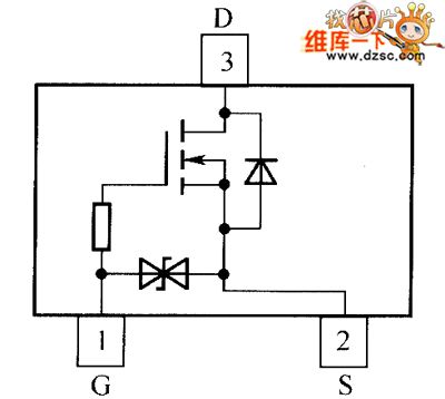
View full Circuit Diagram | Comments | Reading(492)
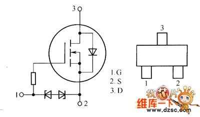
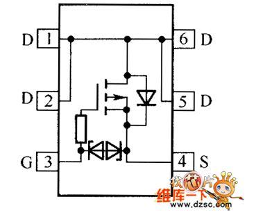
NTJS4405N Internal Circuit
Published:2011/5/3 1:39:00 Author:Felicity | Keyword: Internal Circuit,
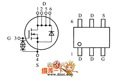
NTJS4405N Internal Circuit is showed in the picture above.
(View)
View full Circuit Diagram | Comments | Reading(536)
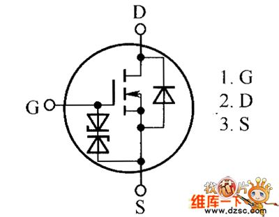
NTGD1100L、NTJD1155L Internal Circuit
Published:2011/5/3 2:51:00 Author:Felicity | Keyword: Internal Circuit,
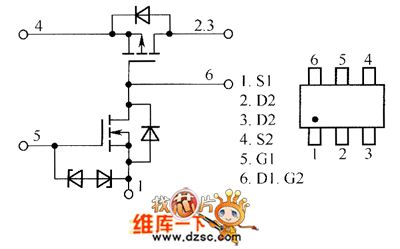
NTGD1100L、NTGD1155L Internal Circuit is showed in the picture above. (View)
View full Circuit Diagram | Comments | Reading(760)
NTJD2152P、NTJD4152P Internal Circuit
Published:2011/5/3 2:47:00 Author:Felicity | Keyword: Internal Circuit
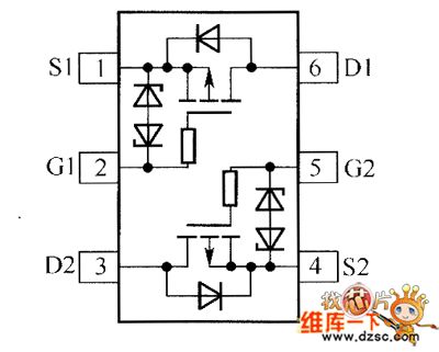
NTJD2152P、NTJD2152P Internal Circuit is showed in the picture above. (View)
View full Circuit Diagram | Comments | Reading(542)
TBA820L, TBA820M, TBA820MS low-frequency B power amplifier integrated circuit
Published:2011/5/3 2:09:00 Author:TaoXi | Keyword: low-frequency, B, power amplifier
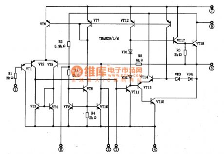
The TBA820L, TBA820M, TBA820MS always use as the low-frequency B power amplifier. It can be used in the cassette tape recorders, compact stereo cassette players, computer sound systems.etc.
1. TBA820L, TBA820M, TBA820MS Pin functions and In-circuit
Electrical parameters and the internal equivalent circuits of the TBA820L, TBA820M, TBA820MS are the same, the internal circuit is as shown in figure 1. They are in the 0 pin double row package, the pin functions and data is shown as the table 1.
Table 1. The pin functions and data of the TBA820L/M/MS
2.TBA820L/M/MS main electrical parameters
(1)Limit conditions: power voltage Vcc=16V, Allowed power PD=1W; Output peak current Io=1.5A
(2)Main electrical parameters: In RL = 8Ω, f = lkHz condition, the main electrical parameters are as shown:
* Static current I (OQ) Maximum value: l2mA, Typical value: 4mA.* Power supply voltage Vcc Maximum value: l6V, Minimum value: 3V, Typical value: 6V, 9V, 12V.* open-loop voltage gain G (VO) G(VO)=75dB; when the closed-loop voltage gain is Ri=33Ω, G(VO)=34dB.* Output power Po cc=9V,THD=l0%: maximum Po=1.2W, minimum Po=0.9W.* Harmonic Distortion THD Po=5OOmW,Ri=33Ω: THD=0.8%(Typical)* Input Resistance Ri pin-3's input resistance is 5MΩ.
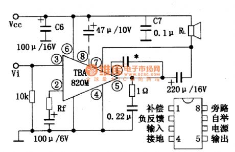
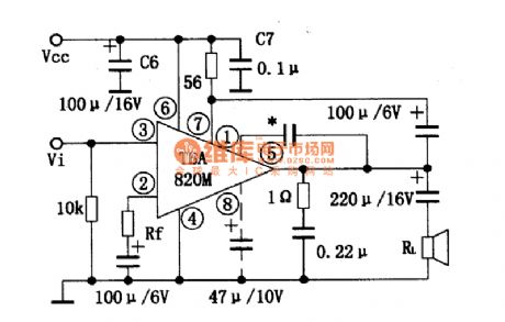
3.TBA82OL/M/MS Typical Application Circuit
The two kinds of typical application circuit are as shown in figure 2 and figure 3. The former's load is connected to the power. The latter's load is connected to the ground.
Figure2 The typical application circuit of the TBA82OL/M/MS manifold
(View)
View full Circuit Diagram | Comments | Reading(4615)
Principle Circuit of Headphones
Published:2011/5/3 2:38:00 Author:Felicity | Keyword: Principle Circuit of Headphones,
Principle Circuit of Headphones is showed in the picture above. (View)
View full Circuit Diagram | Comments | Reading(625)
Principle Circuit of Mixer with 6 Input Channels
Published:2011/5/3 2:30:00 Author:Felicity | Keyword: Principle Circuit of Mixer with 6 Input Channels,
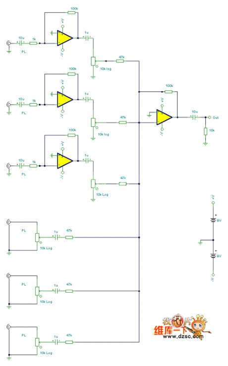
Principle Circuit of Mixer with 6 Input Channels is showed in the picture above. (View)
View full Circuit Diagram | Comments | Reading(622)
NTJS3151P Internal Circuit
Published:2011/5/3 2:03:00 Author:Felicity | Keyword: Internal Circuit,
NTJS3151P Internal Circuit is showed in the picture above. (View)
View full Circuit Diagram | Comments | Reading(501)
Differential Amplifier Circuit
Published:2011/5/3 1:57:00 Author:Felicity | Keyword: Differential Amplifier Circuit,
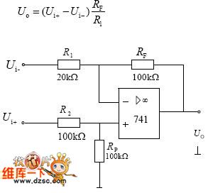
The way of differential connection: the input signal of differential amplifier circuit is inputed from integrated operational amplifier's phase and RP. If the feedback resistanceRF equals to the input resistance, in-phase input voltage minus phase input voltage is the the output voltage. This circuit is also called subtraction circuit. (View)
View full Circuit Diagram | Comments | Reading(586)
High input impedance broadband amplifier circuit diagram composed of field effect pair transistor
Published:2011/5/2 22:46:00 Author:Nicole | Keyword: impedance, broadband, amplifier, field effect, pair transistor
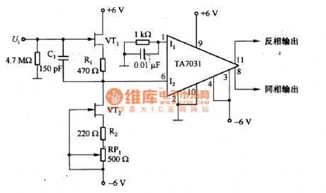
The figure 1 is as shown, it is a high input impedance broadband amplifier which is composed of field effect pair transistor. In the circuit, field effect pair transistor VT1 is connected to VT2, VT2 is as constant current source, UGS's drift of VT1 is decided by R1, then the input is equal to output voltage, the single terminal output is added to the differential amplifier TA7031. Compared this circuit's frequency characteristic to TA7031's frequency characteristic, it is dropped less than 1dB nearby lOMHz, the maximum output voltage is 3V. C1 is feedforward compensation capacitance.
(View)
View full Circuit Diagram | Comments | Reading(726)
| Pages:234/250 At 20221222223224225226227228229230231232233234235236237238239240Under 20 |
Circuit Categories
power supply circuit
Amplifier Circuit
Basic Circuit
LED and Light Circuit
Sensor Circuit
Signal Processing
Electrical Equipment Circuit
Control Circuit
Remote Control Circuit
A/D-D/A Converter Circuit
Audio Circuit
Measuring and Test Circuit
Communication Circuit
Computer-Related Circuit
555 Circuit
Automotive Circuit
Repairing Circuit