
Index 123
Capacitance Filter Circuit
Published:2011/8/23 23:41:00 Author:Robert | Keyword: Capacitance, Filter
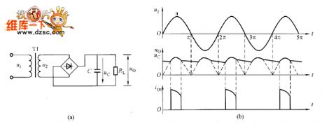
After the rectifier the output voltage would change to be DC voltage, but the voltage waveform fluctuate largely. In order to get the smoothing DC voltage waveform, it needs to use the filter method. The filter method is always using the performance of the reactance feature from the reactance components to the AC signals. And it would connect the capacitance or inductance to the load resistance to make up the filter circuit.The picture shows the single-phase half-wave rectifier capacitance filter circuit and working waveform. From the picture (a), when the circuit is not connectted to the capacitance C, the output voltage would be shown in dotted line of picture (b). (View)
View full Circuit Diagram | Comments | Reading(745)
Inductance Filter Circuit
Published:2011/8/23 23:41:00 Author:Robert | Keyword: Inductance, Filter
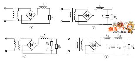
The capacitance filter circuit's output internal resistance is very big. When the RL changing, the port voltage would also change. Also, the when current-limiting diode is conducted, the impact current is very large which would effect its life. The resistance is small but its AC impedance is very large, that is the inductance filter circuit. So it could use the inductance coil for DC voltage, which is the inductance filter. The picture shows some inductance filter circuit.
The picture shows the inductance filter circuit.
The picture (a) shows the single inductance filter circuit. Its weakness is: generally its filter coefficient (the filter coefficient is the first harmonic voltage amplitude ratio between the filter circuit input port and output port) could only be made under several dozens. (View)
View full Circuit Diagram | Comments | Reading(826)
Transistor Basic Voltage Regulator Circuit
Published:2011/8/23 23:40:00 Author:Robert | Keyword: Transistor, Basic, Voltage, Regulator
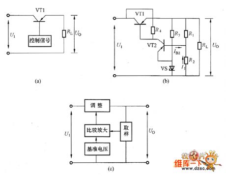
The transistors series voltage regulator circuit is shown in the picture. And, the picture (a) is equivalent circuit. The VT1 is adjustment transistor which is used to adjust the output voltage. The VT1 and load RL are in series. So this circuit is called the series voltage regulator circuit. Because the adjustment tube is using the transistors, the transistor series voltage regulator circuit could work under a big working current which could overcome the weakness that the zener diode regulator circuit's output current is limited by the zener diode limiting current. The picture (b) is the practical series voltage regulator circuit. The picture (c) is its diagram circuit. (View)
View full Circuit Diagram | Comments | Reading(1088)
Voltage Adjustable Circuit
Published:2011/8/23 23:41:00 Author:Robert | Keyword: Voltage, Adjustable
The modern mobile electronic devices is more easier to have this problem than the inchoate devices. In the communication devices and the FM radio, the oscillator voltage is controlled specially. The picture (a) shows the zener diode controller which is used in many car radio circuits. The picture (b) shows a three-segment voltage controller. It could control the mobile transmitter oscillator voltage in 10V. If these controlling components have errors, the circuit would have the frequency drifting. So that the nominal 12V car power is practically unstable. (View)
View full Circuit Diagram | Comments | Reading(682)
Grid Electrode Driving Circuit With Shortening Turn-Off Time
Published:2011/8/23 23:39:00 Author:Robert | Keyword: Grid, Electrode, Driving, Shorten, Turn-Off, Time
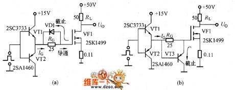
The picture shows the grid electrode driving circuit with shortening power MOSFET turn-off time. In the circuit shown in picture (a), the transistor VT1 and VT2 are make up the push-pull driving circuit with low output impedance. When the VF1 is conducted and the VD1 is disconnected, it would be through the grid resistance RG to charge the VF1's input capacitance Ciss. The RG limits its peak current. The VF1 turn-off time driving circuit would absorb the grid current and the diode VD1 would be conducted to short the RG. Thus the Ciss would discharge with a large current. So the electric charge stored in the grid electrode would be released rapidly.
The picture shows the grid electrode driving circuit with shortening turn-off time. (View)
View full Circuit Diagram | Comments | Reading(1173)
Push-Pull Switching Circuit With Grounding Source Electrode
Published:2011/8/23 23:39:00 Author:Robert | Keyword: Push-Pull, Switching, Grounding, Source, Electrode
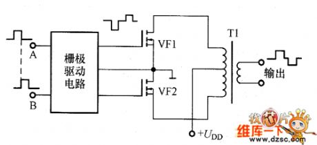
In the large-power applications it usually uses the push-pull switching circuit with transformer middle tapping method. The picture shows the common-used push-pull circuit with grounding source electrode. The push-pull switching circuit's input and output's phase difference is 180°. But the switching power controller has the A phase and the B phase which also have the 180° phase difference, it could directly drive the push-pull switching circuit composed of power MOSFET. Also in no-load case the power MOSFET in the circuit would have a high voltage between its drain electrode and source electrode which would easily have breakdown. So the power MOSFET's withstand voltage must have enough surplus capacity, and also it needs the absorbing circuit to limit the surge voltage. (View)
View full Circuit Diagram | Comments | Reading(757)
Transistor Disconnecting Circuit Using Inductance Stored Energy
Published:2011/8/23 23:39:00 Author:Robert | Keyword: Transistor, Disconnecting, Inductance, Stored, Energy
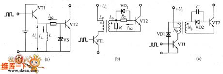
The picture shows the transistor disconnecting circuit using inductance stored energy. In the circuit shown in picture (a), during the transistor VT1 conducted time, the current IL, which is through the inductance L is IL, would change to be the peak current Ip after the VT1 conducting. Ip=U1TON/Lo. When the VT1 is disconnected, for keeping the current, the reverse current Ib2, which is through the VT2 base electrode, peak current would be Ip. This would accelerate the VT1's switching time. For this kind of circuit, because the reverse current Ib2 and the transistor conducted time TON are proportional, it would not get enough reverse current when the pulse is narrow. (View)
View full Circuit Diagram | Comments | Reading(644)
Temperature monitoring circuit composed of the AD590
Published:2011/8/17 21:05:00 Author: | Keyword: Temperature, monitoring circuit
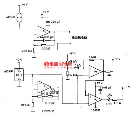
The temperature monitoring circuit which is composed of the AD590 is as shown in the figure, it uses the 9V battery as the power supply. In this circuit, A1 is the current/voltage conversion and voltage amplifier circuit, the monitoring temperature range is -50 to +150℃, the output port of A1 is connected with the positive input port of the digital multimeter (monitor circuit). A2 is the O℃ benchmark and temperature correction circuit, the output port of it is connected with the negative input port of the digital multimeter. The AD580 is one kind of precision voltage reference device, it supplies the reference voltage to the A2-A4. The MD590 has the correction error, this has the relationship with the device level, you can use the RP1(500Ω) fine-tuning potentiometer to eliminate the error when the temperature is 25℃.
(View)
View full Circuit Diagram | Comments | Reading(1428)
Temperature measurement circuit composed of the platinum RTD
Published:2011/8/23 22:29:00 Author: | Keyword: Temperature measurement, platinum RTD
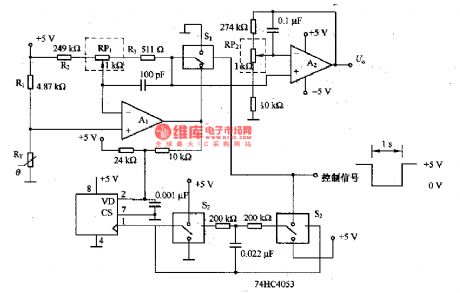
The temperature measurement circuit which is composed of the platinum RTD is as shown in the figure 3-14. In this circuit, the RT is used as the temperature sensor, it is designed as one kind of 100Ω(25℃) platinum RTD. This kind of platinum RTD has high stability and very high precision temperature coefficient, so the +5V power supply supplies the 1mA current to the RT through R1, and we can get the relationship between the temperature and output signal voltage, if the temperature changes 1℃, the circuit will produce -385μV signal voltage. The proportion type measuring bridge circuit is composed of the R2, RP1 and R3, A1 is the bridge circuit amplifier which can be used as the digital control potentiometer of the feedback component to capture and keep the initial reference temperature T0 automatically.
(View)
View full Circuit Diagram | Comments | Reading(2208)
Multi-functional vision protector circuit
Published:2011/8/23 22:29:00 Author: | Keyword: Multi-functional, vision protector
The Multi-functional vision protector circuit
(a) is the infrared transmitter circuit; (b) is the infrared receiver circuit
(View)
View full Circuit Diagram | Comments | Reading(995)
Half wave mode synchronous wave-detection circuit
Published:2011/8/23 22:25:00 Author: | Keyword: Half wave mode, synchronous, wave-detection
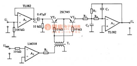
The Half wave mode synchronous wave-detection circuit is as shown in the figure. This is the basic mode of the synchronous wave-detection, the output voltage U=Umcosφ, and we can get the signal amplitude of Um and phase position φ. The A1 is the buffer amplifier, the output impedance is very low. C1 is the stopping condenser, it can prevent the imbalance of A1 or the drifting to affect the performance of the circuit. A2 is the zero-cross comparator, it need to use the fast conversion speed op amp, or there will be the phase delay. The switching circuit is composed of the VT1 and VT2. The transformer T1 can make the switching signal in the floating ground state. The R1 can be used to adjust the amplitude of the switch driving signal.
(View)
View full Circuit Diagram | Comments | Reading(722)
Switching type voltage transform integrated circuit
Published:2011/8/23 22:26:00 Author: | Keyword: Switching type, voltage transform, integrated circuit
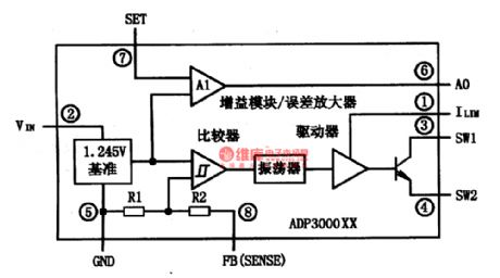
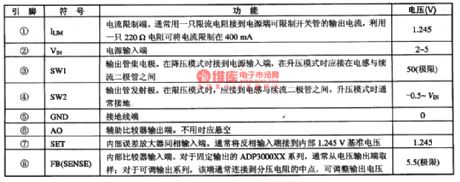
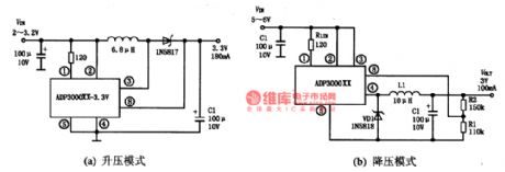
The ADP300OXX is designed as the new micro power consumption type DC/DC converter that is produced by the ANALOG DEVICES company, and it can be used in the carrier communication equipments and the bus power supply equipments.
1.Features
The ADP300OXX is the series product, the non-suffix output voltage can be adjusted, the output voltage of the ADP300OXX-3.3 is 3.3V, the output voltage of the ADP300OXX-5 is 5V, the output voltage of the ADP300OXX-l2 is 12V. And this device can be used in the voltage step-up or step-down application. The typical conversion efficiency is 80%, the switching frequency is 400kHz, and it also has the low voltage detection circuit. The internal circuit block diagram of the ADP300OXX series is as shown in the figure.
2.Pin functions and data
The ADP300OXX series IC uses the DIP-8 or SOIC-8 package, the pin functions and data are as shown in the table 1.
3.Typical application circuit
(View)
View full Circuit Diagram | Comments | Reading(611)
The synchronous wave-detection circuit composed of the MCI496L
Published:2011/8/23 22:26:00 Author: | Keyword: synchronous, wave-detection
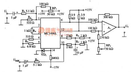
The synchronous wave-detection circuit composed of the MCI496L is as shown in the figure. The MCI496L is the differential circuit that is composed of the geminate transistor, the output uses the collector electrode open-circuit mode, you need to add the load resistor with it if you want to use it. The 3-time gain level shift circuit is composed of A1, the RP2 can be used to adjust the offset voltage to ensure the differential balance.
When the input signal is larger than 300mV, the internal differential amplifier of MCI496L will be in the saturated state, so at the signal input Vi port and the benchmark phase input UREF port, the attenuation network is composed of the R1, R2 and R3. So the input signal of the MCI496L can be a few volts.
(View)
View full Circuit Diagram | Comments | Reading(677)
Broadband level wave-detection circuit
Published:2011/8/23 22:26:00 Author: | Keyword: Broadband level, wave-detection
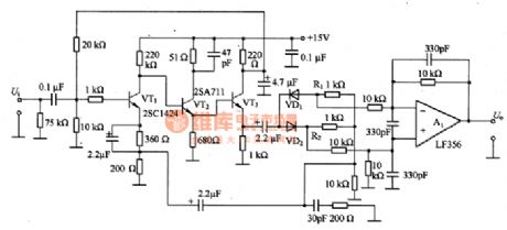
The broadband level wave-detection circuit is as shown in the figure. This circuit is the broadband amplifier that is composed of the transistor, and you can connect the rectifier diode with the negative feedback loop to form the 1OMHZ, good linearity level detection circuit. In this circuit, the VT1~VT3 use the high cut-off frequency T transistor, and these transistors can form the directly coupled type amplifier circuit; the full wave rectifier circuit is composed of the diodes VD1 and VD2; the resistances R1 and R2 have the feedback function, the A1 has the differential/single polarity conversion function.
(View)
View full Circuit Diagram | Comments | Reading(695)
Simple pulse width modulation circuit
Published:2011/8/23 22:27:00 Author: | Keyword: Simple, pulse width, modulation
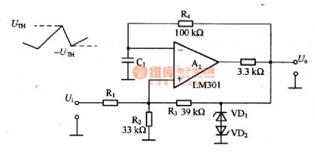
The simple pulse width modulation circuit is as shown in the figure. It uses the operational amplifier to form the multivibrator, so we can get the positive and negative symmetrical oscillation output signal with the duty ratio of 50%. If we change the threshold voltage from external, we can realize the pulse width modulation. If this circuit is not connected with the resistor R1, the oscillation frequency f0 is decided by the cycle of the hysteresis voltage, f0=1/2R4C1ln(1+(2R2/R3)).
If [1+(2R2/R3)]=2.718, the f0=l/(2R4C1), so we can change the duty ratio by using the external voltage to move the ±UTH through R1.
(View)
View full Circuit Diagram | Comments | Reading(2365)
Mazda 96PROBE air conditioning warm wind circuit
Published:2011/8/23 22:24:00 Author: | Keyword: Mazda, air conditioning, warm wind
The Mazda 96PROBE air conditioning warm wind circuit is as shown in the figure:
(View)
View full Circuit Diagram | Comments | Reading(651)
Composition of F033 the photosensitive signal amplifying circuit diagram
Published:2011/8/22 22:13:00 Author:Rebekka | Keyword: Photosensitive Signal
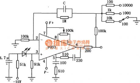
Sensitive signal amplification circuitis used toamplify photodiode or phototransistor optoelectronic devices such as electrical signals. When the incident light illumination changes, the optical devicecan generate certain current, because the signal is very weak sensitive, so it’s better to use a operational amplifier in very low input bias current. In order to eliminate oscillations, it adds a small capacitor C (pF orders of magnitude) in the feedback circuit, but the value of C affects the bandwidth of the amplifier. The DC gain of the circuit is l00, 1000,10000, you can select switch corresponding to 10kΩ, 1kΩ, 100Ω resistors to ground, the circuit of the resistor accuracy must be better than ± 1%. Photocell uses FPT102 or FPT100. (View)
View full Circuit Diagram | Comments | Reading(640)
AC power supply monitoring circuit composed of the 74HC123
Published:2011/8/14 20:27:00 Author:TaoXi | Keyword: AC, power supply, monitoring
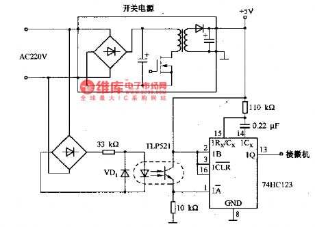
The AC power supply monitoring circuit composed of the 74HC123. When the AC power is cut off, the important data that is storaged in the microcomputer might disappear. So we need to add the power transient breaking detection circuit to protect the data in the memorizer. The AC220V voltage is rectified and stabilized to be the +5V ouptut voltage, the voltage can be used as the operating power of the microcomputer, and also it is the operating power of the timer 74HC123 (the 13-pin of the 74HC123 is connected with the microcomputer). When the AC power is normal, the 74HC123 timer will reset to output the high level, the microcomputer operates normally.
(View)
View full Circuit Diagram | Comments | Reading(2255)
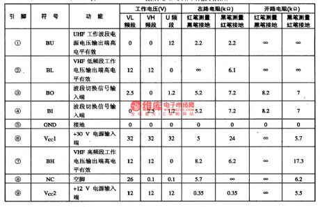
AN5071 frequency band switching control integrated circuit
Published:2011/8/11 19:53:00 Author:TaoXi | Keyword: frequency band, switching, control, integrated circuit
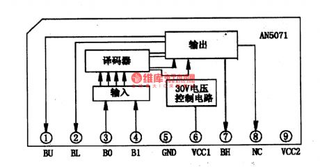
The AN5071 is designed as the frequency band switching control integrated circuit which is produced by the Panasonic company, and it can be used in all kinds of screen color TV sets.
1. The internal circuit block diagram
The AN5071 has three channels of electronic switch and the 30V voltage-stabilizing circuit, the internal circuit block diagram of the manifold is as shown in figure 1-15.
2.Pin functions and data
The AN5071 uses the 9-pin single row package, the pin functions and data of the integrated circuit is as shown in table 1-14.
Table 1-14 The pin functions and data of the AN5071 (View)
View full Circuit Diagram | Comments | Reading(1670)
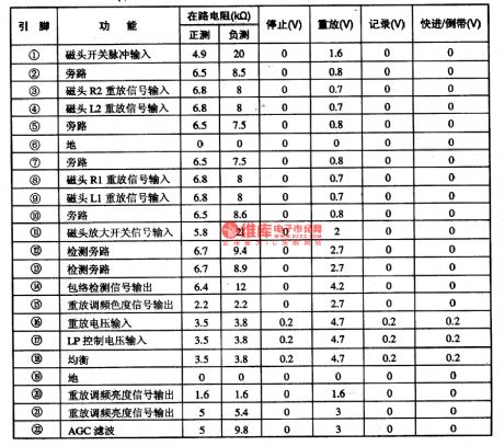
AN3311S camera video magnetic read head replay integrated circuit
Published:2011/8/11 20:17:00 Author:TaoXi | Keyword: camera video, magnetic read head, replay integrated circuit
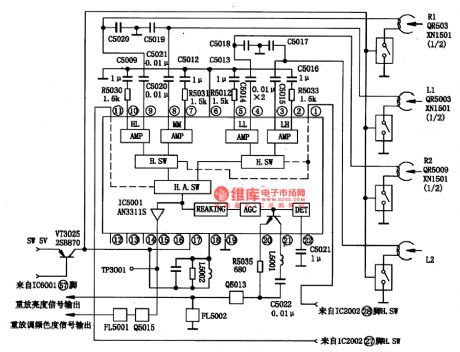
The AN3311S is designed as the camera video magnetic read head replay integrated circuit which is produced by the Panasonic company that can be used in the Panasonic series camera.
The AN3311S integrated circuit has the 4 magnetic read head preamplifier, the magnetic read head switching switch, the envelope comparator, the peak value amplification circuit, the color changing amplification circuit, the AGC amplification circuit. The internal circuit block diagram and the typical application circuit is as shown in figure 1-14, the pin functions and data is as shown in table 1-13.
Table 1-13 The pin functions and data
(View)
View full Circuit Diagram | Comments | Reading(737)
| Pages:123/471 At 20121122123124125126127128129130131132133134135136137138139140Under 20 |
Circuit Categories
power supply circuit
Amplifier Circuit
Basic Circuit
LED and Light Circuit
Sensor Circuit
Signal Processing
Electrical Equipment Circuit
Control Circuit
Remote Control Circuit
A/D-D/A Converter Circuit
Audio Circuit
Measuring and Test Circuit
Communication Circuit
Computer-Related Circuit
555 Circuit
Automotive Circuit
Repairing Circuit