
Index 136
220_MICROSEC_PHANTASTRON_DELAY
Published:2009/7/14 23:41:00 Author:Jessie
Timing accuracy of 1% is achieved by adding temperature-correcting features to basic solid-state circuit.-S. R. Parris and D. A. Staar. Highly Accurate Phantastron Delay Circuit Electronics.33:43,P72-74 (View)
View full Circuit Diagram | Comments | Reading(658)
RTTY_FROM_SATELLITE
Published:2009/7/14 23:40:00 Author:Jessie
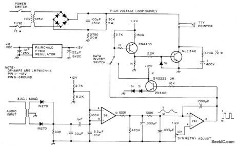
Developed for receiving RTTY transmitted from satellite as space-only keying. Receiver can be operated in CW or narrow-filter mode, to increase signal-to-noise ratio. Any receiver having CW filter with 400-Hz bandwidth can be used. Tune for audio output of 1 kHz. Audio is converted to varying DC voltage by envelope detector and amplified by 741 opamp that drives additional filter having high-level output for space and low-level output for mark. Slow rise and fall times of varying voltage are converted to ON/OFF keying signals by 741 used as comparator, for feeding to two-stage driver and high-voltage loop keying circuit of conventional design.-K.O. Learner and W. A. Kotras, Oscar RTTY Converter, 73 Magazine. July 1975, p 53-54. (View)
View full Circuit Diagram | Comments | Reading(1236)
10_MHz_FUNCTION_GENERATOR
Published:2009/7/14 23:39:00 Author:Jessie
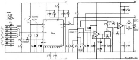
This circuit is built around the MAX038 IC and can provide sine, square, and triangle waveforms from 10 Hz to 10 MHz. PC-board layout techniques suitable for 50 MHz or higher should be used for best results with this circuit. (View)
View full Circuit Diagram | Comments | Reading(3264)
SIMPLE_PULSE_GENERATOR
Published:2009/7/14 23:37:00 Author:Jessie
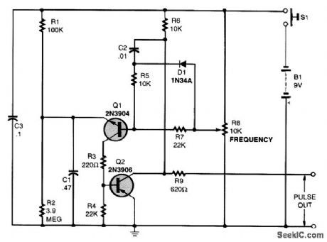
Timing capacitor C1 is charged by battery B1 through R1 until Q1 is forward-biased and starts conducting. When this occurs, a forward base bias is applied to Q2 through Q1 and R3. As Q2 starts conducting, a pulse is made across collector load R6, which is coupled back to Q1's base through C2 and series resistor R5. That drives Q1 to rapidly discharge C1, and then the cycle starts over. In essence, Q1 and Q2 form a high-gain amplifiers, with C2 providing positive feedback. Diode D1 reduces C2's recovery time, while R8 establishes Q1's base bias level. Thus, it is the point at which timing capacitor C1 charges before feedback and capacitor discharge are initiated. The lower Q1's initial base bias, the higher the circuit's repetition rate. Resistor R8, therefore, serves as a frequency control, providing nine octaves of coverage. The circuit will work from 5 to 25 V, but a 9-V source is optimum. Output impedance is 600Ω. A sawtooth signal suitable for use as a linear scope sweep is available across C1. For frequency-divider, sweep-generator, and time-marker uses, synchronization pulses can be applied to Q1's base through a small capacitor. The frequency range can be shifted by using other values for C1 and C2. With values of 100μF for C1 and 3μF for C2, the circuit will work down to about 1/20 Hz. (View)
View full Circuit Diagram | Comments | Reading(1267)
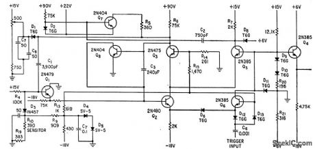
PREFERRED_PHANTASTRON_DELAY
Published:2009/7/14 23:35:00 Author:Jessie
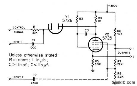
Accepts 20 to 280V control signal, 15-V negativepulse at input 1, and 20-V positive pulse at input 2. Output is +60V, and output is -10V. R3 can be 1 to 3.3 meg and C3 100 to 1,200pf, depending on minimum and maximum duration desired.-NBS, Handbook Preferred Circuits Navy Aeronautical Electronic Equipment, Vol. I, Electron Tube Circuits, 1963 PC 56, p56-2. (View)
View full Circuit Diagram | Comments | Reading(604)
CODED_LOCK
Published:2009/7/14 23:33:00 Author:Jessie
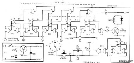
Five-digit combination lock uses five low-cost ICs operating from 5-V supply that can be derived from 12-V auto battery as shown in inset. Six set/reset bistable circuits are formed by cross-coupling pairs of dual-input NAND gates, so 0-V input is needed to change state of each. Five of bistables serve for combination, and sixth prevents operation by number in incorrect sequence. After S1 is set to one number of code, S2 is pushed to enter that number, with process being repeated for other four numbers of combination. Final correct number sets B5 and turns on Tr1, to operate relay that can be used to open door.-S. Lamb, Simple Code-Operated Switch or Combination Lock, Wireless World, June 1974, p 196.
(View)
View full Circuit Diagram | Comments | Reading(1363)
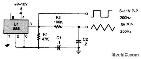
DESIRED_WAVEFORM_GENERATOR
Published:2009/7/14 23:33:00 Author:Jessie
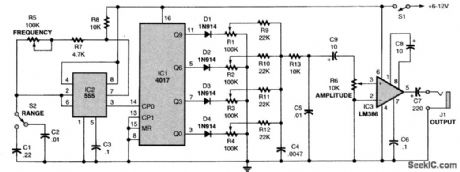
This is a filtered step-function generator in which the wave amplitude at each step is set by a linear potentiometer (R1to R4).With the potentiometers arranged in time order and side by side (the way they are in a graphic equalizer), the positions of the knobs describe the output waveform. The 555 oscillator, controlled by R5 and C0 or C2, sets the duration of each step, and (there-fore) also the wave frequency. Potentiometer R5 controls the step frequency and the capacitors define the frequency range. The output of the 555 is applied to the clock input for the 4017 decimal counter, which activates its outputs one at a time. The linear potentiometers divide the voltage of each output, and thus determine the output voltage at a given step point. The schematic shows potentiometers only in Q0, Q3, Q6, and Q9, but for smoother waveforms potentiometers should be at all of the outputs, except the CARRY-OUT pin. The composite waveform is now purified by the filter formed by R13, C4, and C5, so the output will be rounded. The amplitude is controlled by the LM386 audio amplifier's input. For high frequencies, replace the amplifier with a 741 or some other high-frequency op amp. (View)
View full Circuit Diagram | Comments | Reading(1573)
12_V_OVERVOLTAGE_LIMITER
Published:2009/7/14 23:31:00 Author:Jessie
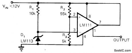
Single LM111 comparator is basis for simple overvoltage protection of circuits drawing less than 50mA. Fraction of input supply is compared to 1.2-V reference. When input exceeds reference level, power is removed from output.-R. C. Dobkin, Comparators Can Do More than Just Compare, EDN Magazine, Nov. 1, 1972, p 34-37. (View)
View full Circuit Diagram | Comments | Reading(1019)
HIGH_INPUT_IMPEDANCE
Published:2009/7/14 20:52:00 Author:May
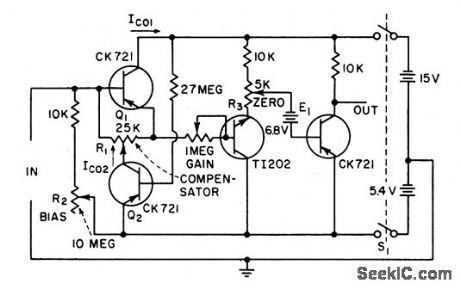
Gives current gain of 1,000, voltage gain of 40, input impedance of0.4 meg, and good short-term temperature stability. Output stage is battery-coupled.-D. Schuster, D-C Transistor Amplifier for High-Impedance Input, Electronics, 31:9, p 64-66. (View)
View full Circuit Diagram | Comments | Reading(0)
SIMPLE_TRIANGLE_WAVEFORM_GENERATOR
Published:2009/7/14 23:30:00 Author:Jessie
This triangle-waveform generator was designed to give good results with as few parts as possible. (View)
View full Circuit Diagram | Comments | Reading(1835)
EQUIPMENT_INTERFACE_PROTECTION
Published:2009/7/14 23:29:00 Author:Jessie

When circuit shown is used to transfer signal from one piece of equipment to another, desired signal passes with very little degradation. Component values can be chosen to make thyristor SCP1 latch at any desired voltage between A and B that is greater than 0V, blowing fuse F1 and giving desired protective isolation. On other side of circuit, SCR2 will latch and blow F2 when voltage exceeds limiting value set by diode D2 and zener D4. Zeners are 10-V CV7144, diodes are CV9637 small-signal silicon, resistors are 10K, capacitors are 0.047 μF, and thyristors are 2N4147.-S. G. Pinto and A. P. Bell, Thyristor Protection Circuit, Wireless World, Oct. 1975, p 473. (View)
View full Circuit Diagram | Comments | Reading(767)
CURRENT_MODE_LOGIC_FOR_500_MC_GATED_FLIP_FIOP
Published:2009/7/14 20:51:00 Author:May
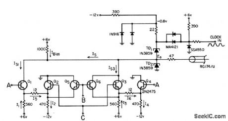
Uses 2N2475 Transistors and 1N3859 tunnel diodes in current mode logic circuit having four inputs that can be energized to provide variety of desired logic functions. Supply of 0.8 v is obtained by passing current through two forward silicon diodes. Narrow 1-nsec clock pulse is generated by snap diode as close as possible to tunnel diode.-R. Glasgal , 500 MHz Transistor-TD Gated Flip Flop, EEE, 14:1, p 98-101. (View)
View full Circuit Diagram | Comments | Reading(839)
ATTACK_DECAY_RAMP_GENERATOR
Published:2009/7/14 23:29:00 Author:Jessie
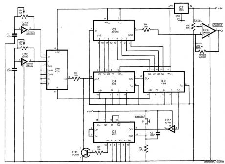
In the circuit diagram shown, a digital-to-analog converter (DAC) IC is used to create an envelope waveform, the attack and decay of which are controllable. Typical applications can include audio and music synthesizer circuitry. Its operation is as follows. IC1a and IC1b form two variable-frequency oscillators, whose outputs are fed to IC2. This is configured as a demultiplexer, addressed by a signal appearing on pin 11. The signal from IC1a or IC1b appears at the output, pin 3. Initially pin 11 of IC2 will be high, so IC1a will be selected and fed through resistor R1 to IC4, a bi-nary counter, which is cascaded to 106. In total, this results in an 8-bit binary count (0 to 255) appearing at the counters' outputs. The speed of the count is adjustable with VR1. The counter output is fed directly to IC3, a ZN429E digital-to-analog converter. The ramp voltage appears at pin 4 of IC3, and will always be between 0 and 4 V. When the counter reaches its terminal count of 255, pin 7 of IC6 (CARRY OUT) will go low. This signal is inverted by IC1c and used as a clock pulse to IC5, a 4013 D-type flip-flop. The output at pin 1 of IC5 now goes low, so that a logic 0 is placed on pin 11 of IC2 and on pin 10 (UP/DOWN) of both counter ICs. Oscillator IC1b is now fed through the dernultiplexer to the counters, which now count down from 255. The output voltage from IC3 will now fall at a rate determined by the setting of VR2. As the count passes zero and rolls back to 255, a pulse again appears at pin 7 of IC6, and the cycle continues. At any time, switch S1 (debounced by CB and R3) can be momentarily activated. This causes a high output at pin 13 of IC5, which drives transistor TR1, shunting the clock signal to the counters. This will freeze the count at that point. A second operation of S1 restarts the count from where it left off. A buffer/amplifier formed by IC8a (one half of an LM358N) allows the output voltage of the DAC (IC3) to be increased or the dc level shifted. (View)
View full Circuit Diagram | Comments | Reading(1899)
FAIL_SAFE_TTL_INTERFACE
Published:2009/7/14 20:51:00 Author:May
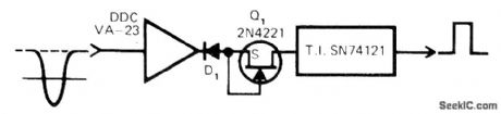
Diode and FET protect SN74121 high-speed level detector from excessive opamp output voltage. If input of opamp goes too far negative, positive-going output will cause breakdown of TTL input. Protective interface makes circuit fail-safe without loss of operating speed. D, should be highspeed germanium diode with breakdown volt-age above highest positive output of amplifier (usually about 15 V).-K. I. Wolfe, A Safer Analog-to-Digital Interface, EDN Magazine, March 5, 1974, p 74. (View)
View full Circuit Diagram | Comments | Reading(723)
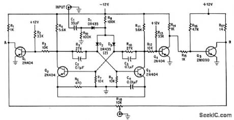
NOR_FUNCTION_RESET
Published:2009/7/14 20:49:00 Author:May
Modified flip-flop is set or reset when all input signals are low, corresponding to nor-function of input signals rather than the usual or function,-L. Mercurio, Flip-flop Operated by Input Signal NOR, EEE, 3:12,p 65. (View)
View full Circuit Diagram | Comments | Reading(739)
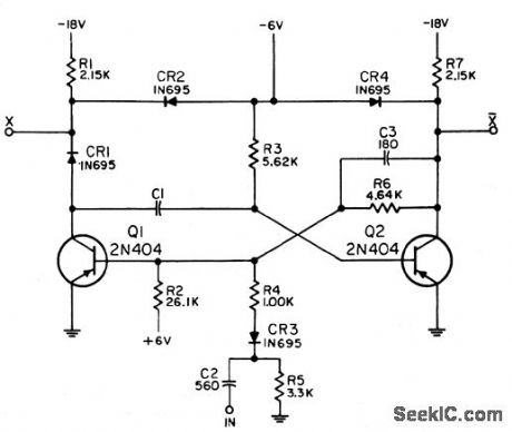
STARTER_FOR_FLIP_FLOP
Published:2009/7/14 20:49:00 Author:May
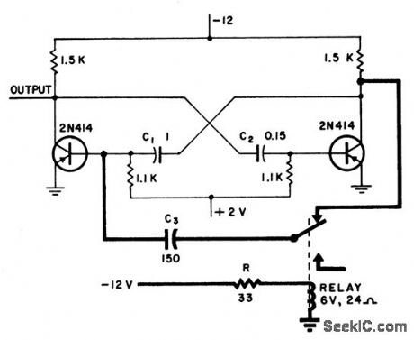
Free-running flip-flop (thin lines) has several desired features but will not start oscillation by itself. Output impedance is less than 1,800 ohms, period is 1 millisec, and circuit is quite stable once in operation. Heavy lines show additions re quired for starting flip-flop when it is stalled.C3 (150 mfd) is in circuit for time period in which power supply voltage increases from 0 to 9 v after switch is dosed. Relay pulls in at 9 v, to remove C3 from circuit after it has served its starting function.-Starter Circuit for Flip-Flop, Electronic Circuit Design Handbook, Mactier Pub. Corp., N.Y., 1965, p 229. (View)
View full Circuit Diagram | Comments | Reading(687)
AUDIO_PROCESSOR_FOR_RTTY_RECEIVER
Published:2009/7/14 23:29:00 Author:Jessie
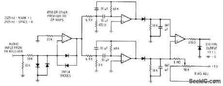
Audio tones of 2125 and 2975 Hz, as received and detected by FM receiver, are limited and fed to two active bandpass filters, each set to one of tone frequencies. Outputs are amplitude-detected and compared, to give output of 1 for 2125 Hz and output of 0 for 2975 Hz. Output is suitable for UART providing serial-to-parallel conversion,-D. Lancaster, TV Typewriter Cookbook, Howard W. Sams, Indianapolis, IN, 1976, p 174-175. (View)
View full Circuit Diagram | Comments | Reading(800)
MONOSTABLE_DELAY
Published:2009/7/14 23:28:00 Author:Jessie
Designed to perform delay function in digital logic circuits for computer, control, and communication equipment. Choice of feedback capacitor C1 gives delay range from 2microsec to 100 millisec.R3 may be made variable for further adjustment of time delay.-NBS, Handbook Preferred Circuits Navy Aeronautical Electronic Equipment, Vol. II, Semiconductor Device Circuits, PSC 10 (originally PC 213), p 10-2. (View)
View full Circuit Diagram | Comments | Reading(877)
BIPOLAR_OUTPUT
Published:2009/7/14 20:48:00 Author:May
Output is dean square wave whose symmetry with respect to ground can be balanced by potentiometer R18. When input is fed by pulse generator, output can be used to test frequency re sponse of transistor circuits.-F. C. Ruegg, Multivibrator Provides Bidirectional Output Pulses, Electronics, 38:17, p 87. (View)
View full Circuit Diagram | Comments | Reading(0)
GROUND_FAULT_INTERRUPTER
Published:2009/7/14 23:27:00 Author:Jessie
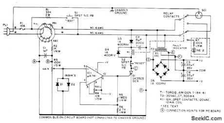
Compares current in ungrounded side of power line with current in neutral conductor. If currents are not equal, ground fault exists because portion of line current is taking an unintended return path through leaky electric appliance or human body. Voltage induced in toroid by unbalanced current is amplified for energizing relay K1 to break circuit. Toroid uses Amidon T-184-41 core, with 600 turns No. 30 for secondary, and 12 turns No. 16 solid twisted-pair for primary. Circuit operates on fault current of 4mA, well below danger limit for children.-W. J, Prudhomme, The Unzapper, 73 Magazine, Nov./ Dec. 1975, p 151-156.
(View)
View full Circuit Diagram | Comments | Reading(1239)
| Pages:136/471 At 20121122123124125126127128129130131132133134135136137138139140Under 20 |
Circuit Categories
power supply circuit
Amplifier Circuit
Basic Circuit
LED and Light Circuit
Sensor Circuit
Signal Processing
Electrical Equipment Circuit
Control Circuit
Remote Control Circuit
A/D-D/A Converter Circuit
Audio Circuit
Measuring and Test Circuit
Communication Circuit
Computer-Related Circuit
555 Circuit
Automotive Circuit
Repairing Circuit