
Index 134
DIRECT_COUPLED_NOR_GATES
Published:2009/7/14 21:21:00 Author:May
Consists of two epitaxial-transistor nor gates.-D. Hall, Using Epitaxial Transistors in Switching and R-F Circuits, Electronics, 34:13, p 52-53. (View)
View full Circuit Diagram | Comments | Reading(678)
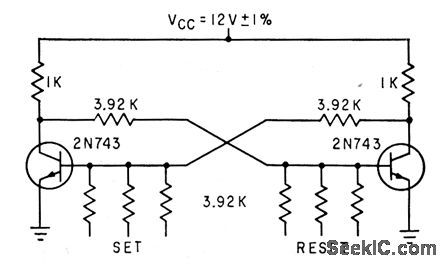
DIRECT_COUPLED_FLIP_FLOP
Published:2009/7/14 21:20:00 Author:May
Typical switching times are 12 millimicrosec for tr and 15 millimicrosec for tf. -Philco MAT Transistors for Logic Circuits up to 5 Mc (Philco ad), Electronics, 33:17, p 50. (View)
View full Circuit Diagram | Comments | Reading(668)
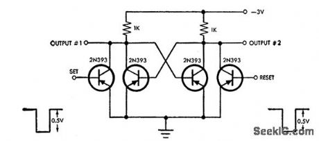
DIODE_COUPLED_FLIP_FLOP
Published:2009/7/14 21:20:00 Author:May
Typical switching limes are 20 millimicrosec for tr and 60 millimicrosec for tf. -Philco MAT Transistors for Logic Circuits up to 5 Mc (Philco ad), Electronics, 33:17, p 50. (View)
View full Circuit Diagram | Comments | Reading(744)
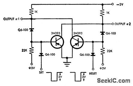
RESISTOR_COUPLED_FLIP_FLOP
Published:2009/7/14 21:19:00 Author:May
Typical switching times are 40 millimicrosec for tr and 110 millimicrosec for tf. -Philco MAT Transistors for Logic Circuits up to 5 Mc (Philco ad), Electronics, 33:17, p 50. (View)
View full Circuit Diagram | Comments | Reading(703)
SOLENOID_PUMP_PULSER
Published:2009/7/14 21:17:00 Author:May
Scr flip-flop feeds 5-amp pulses altenately to two solenoid pump coils at rates varying from 1.5 to 25 cps.-U. L. Upson, Solid-State Pulser Drives Chemical Pump, Electronics, 33:49, p 74-76. (View)
View full Circuit Diagram | Comments | Reading(703)
SELF_INDICATING_FLIP_FLOP
Published:2009/7/14 21:17:00 Author:May
Uses Amperex 6679 triode having fluorescent anode, to eliminate need for neons as indicators. Incorporates collector protection and stabilization against beta variation of transistor.-H. Rodriques deMiranda and I. Rudich, Indicator Triode for Direct Data Readout, Electronics, 33:6, p 52-54. (View)
View full Circuit Diagram | Comments | Reading(678)
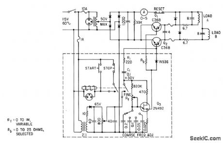
SLOW_MAKE_RELAY
Published:2009/7/14 23:37:00 Author:Jessie
Circuit energizes relay with delay controlled by R2-C1 after driving pulse is applied. Relay de-energizes the instant driving pulse is removed.-P. Haas, Timing Circuits Control Relays, Electronics, 38:6,p85. (View)
View full Circuit Diagram | Comments | Reading(850)
A_F_OUTPUT_TRANSISTOR_PROTECTION
Published:2009/7/14 22:48:00 Author:Jessie
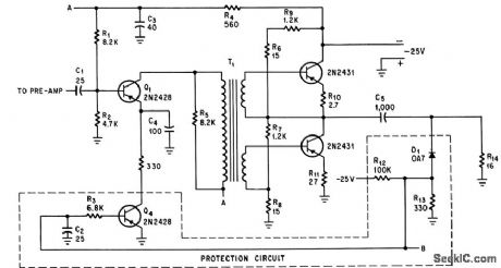
When output of 3-w audio amplifier is short-circuit,protection circuit reduces overall gain by 20 db.-E. Segatis, Circuit Protects Amplifier Against Short Circuit,Electronics,37:23,p 61-62. (View)
View full Circuit Diagram | Comments | Reading(794)
AC_LINE_ZERO_CROSSING_DETECTOR
Published:2009/7/14 22:48:00 Author:Jessie
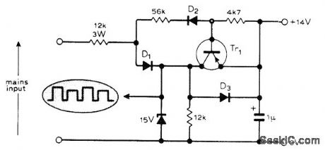
Positive-going half-cycles forward-bias D1, allowing capacitor to charge through D3 to 14V. Negative half-cycles forward-bias D2 allowing capacitor to charge through D3 to 14 V. Negative half-cycles forward-bias D2 to turn on Tr1 and discharge capacitor. Output is about 1 V less on negative half-cycles. Transistor and diode types are not critical, except that D1 must withstand full reverse voltage of AC line.-R. J. Torrens, Zero Crossing Detector, Wireless World, Jan.1977, p 78.
(View)
View full Circuit Diagram | Comments | Reading(1147)
GATE_TURNOFF_SCR_FLIP_FLOP
Published:2009/7/14 21:16:00 Author:May
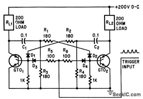
Capacitor-commutated flip-flop transfers current front one load to other each time positive trigger pulse is applied to common input line, at rates up to 10 kc.-D. It. Grafham, Now the Gate Turnoff Switch Speeds Up D-C Switching, Electronics, 37:12, p 64-71. (View)
View full Circuit Diagram | Comments | Reading(1048)
LASER_CURRENT_MODULATION
Published:2009/7/14 11:50:00 Author:May
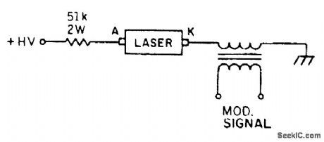
Depending on laser characteristics, only a small percentage of modulation (around 10 percent) is possible with this scheme. (View)
View full Circuit Diagram | Comments | Reading(765)
WEATHER_VANE
Published:2009/7/15 0:22:00 Author:Jessie
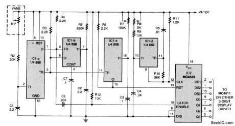
IC1-a and IC1-b form an astable oscillator in which IC1-a produces a positive pulse width that is proportional to the resistance of the segmented potentiometer, R1. The negative pulse width, deter-mined by IC1-b, is fixed. The third section, IC1-c, is triggered by the falling edge of IC1-b. Its pulse width is set by potentiometer R7 so that it is exactly equal to the width of the IC1-a's pulse when the vane is at zero resistance. Potentiometer R8 and IC1-d make up the frequency reference. An astable oscillator (formed out of IC1-d and its surrounding components) provides a clock signal to IC2, a 555 timer IC. The RESET pulse from IC1-c starts to count at zero, and the LATCH pulse from IC1-a freezes the instantaneous reading in the timer. So, U2 counts the time between the falling edge of IC1-a and the falling edge of IC1-c, which is determined by the position of the vane. The timer can feed its digital output to the three-digit display circuit of your choosing (such as an MC4511 display driver). To adjust the circuit, rotate RI (the transducer) to its zero-resistance position (North) and adjust R7 until the readout is zero. Second, rotate R1 to its maximum-resistance position and adjust R8 until the readout is 350. That will give, theoretically, readings between zero and 350 in 10- degree increments as the vane is rotated. (View)
View full Circuit Diagram | Comments | Reading(1725)
ANEMOMETER
Published:2009/7/15 0:18:00 Author:Jessie
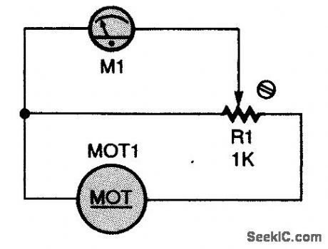
Here is a really simple and inexpensive anemometer. You can use any small dc motor for MOT1. Meter M1 can be any milliampere or microampere meter with markings from 0 to 50 or100. The parts, including the 1000-Ω, 15-tum potentiometer, are available at hobbyist sources. A three-paddle wheel for the motor can be made with golf-ball-sized hollow plastic balls. Cut two of them in half, and bolt three of the halves to a PVC hub, using 6-32 machine screws. Calibrate the circuit by holding it out of a car window while someone drives steadily between 20 and 30 miles per hour on a still day. (View)
View full Circuit Diagram | Comments | Reading(1645)
SFERIC_SIMULATOR_CIRCUIT
Published:2009/7/15 0:14:00 Author:Jessie
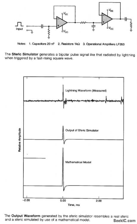
This circuit generates a signal that simulates the waveform of a sferic-the very-low-frequency electromagnetic signals generated by a lightning strike. This circuit is designed to test and calibrate lightning-detecting instruments. Typically, lightning-detecting instruments have been calibrated and tested using single-frequency signals or broadband noise sources, which do not have the spectral characteristics of sferics. This circuit generates a bipolar pulse waveform that closely approximates the main features of sferics. The circuit contains few components. This circuit assembly is light in weight and compact; even a breadboard version could fit in a 1.5-inch square (about 3.8 cm). To ensure that the output waveform has the desired shape, the trigger pulse fed to the input terminal of this circuit must be a square wave with rise and fall times less than 100 ns. To prevent coalescence of sequential output pulses, the square-wave pulse-repetition frequency should be kept at or below 3000 Hz. (View)
View full Circuit Diagram | Comments | Reading(825)
PCM_DECODER
Published:2009/7/15 0:05:00 Author:Jessie
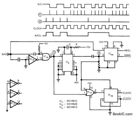
Three CMOS ICs provide decoding of Manchester (split-phase) PCM signals by generating missing mark which should occur NRZL at each change of level data to recover original clock frequency. Retriggerable mono MVBR NHZL times out at slightly longer than half of original clock frequency. Signal levels are TTL-compatible. Values of C and R depend on system frequency. Other resistors are 15K, and other capacitors are 470 pF.-M. A. Lear, M. L. Roginsky, and J. A. Tabb, PCM Signal Processor Draws Little Power, EDN Magazine, April 20, 1975, p 70. (View)
View full Circuit Diagram | Comments | Reading(5080)
PULSE_STRETCHING__MONO
Published:2009/7/15 0:02:00 Author:Jessie
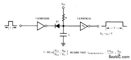
Section of CMOS MM74C04 inverter accepts positive input pulse by going low and discharging C. Capacitor is rapidly discharged, driving input of MM74C14 Schmitt trigger low. Output of Schmitt then goes positive for interval To which is equal to input pulse duration plus interval T that depends on values used for R, C, and supply voltage.- CMOS Databook, National Semiconductor, Santa Clara, CA, 1977, p 5-30-5-35. (View)
View full Circuit Diagram | Comments | Reading(1234)
TWO_STAGE_CASCADED_COMMON_EMITTER
Published:2009/7/15 Author:Jessie
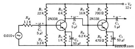
Design procedure is given for low-level amplifierthat is one of the most-used circuits in all transistor applications, for boosting milli-volt-range signals to workable level of several volts. Capacitance coupling isused for ac operation along with d-c stability. Total power gain is 64 db. Voltagegain is 1,000.-Texas Instruments Inc., Transistor Circuit Design, McGraw. Hill,N.Y.,1963, p 198. (View)
View full Circuit Diagram | Comments | Reading(2925)
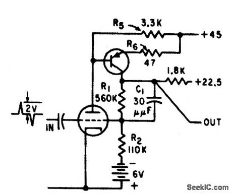
FEEDBACK_PROVIDES_STABILIZATION
Published:2009/7/14 21:11:00 Author:May
Resistor Rf, connected between bases of Q1 and Q2, provides negative feedback to make flip-flop less sensitive to voltage variations and transistor unbalance. Will operate on 3.v pulses having 0.5-microsec fall time. Without feedback, higher voltage would be required for triggering.-P. Cheilik, Feed-back Stabilizes Flip-Flop, Electronics, 31:19, p 91-96. (View)
View full Circuit Diagram | Comments | Reading(616)
SINGLE_TONE_SIGNALING
Published:2009/7/14 21:11:00 Author:May
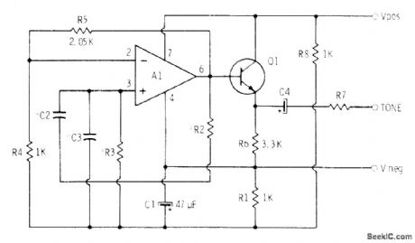
Wien-bridge oscillator using 741 opamp drives 2N2924 or equivalent NPN transistor to generate stable audio tone for signaling over telephone lines Tuning capacitor(C2 and C3 are equal)and resistor(R2 and R3 are equal) values range from 0.1μF and 15.9K for 100 Hz to 0.005 μF and 6.3K for 5000Hz For other frequencies use f =0.159/R2C2 With 12-V supply tone output is about 7 V P-P Select R7 to match impedance of driven circuit.-C. D Rakes. Integrated Circuit Projects. Howard W Sams . Indianapolis IN 1975.p 55-60. (View)
View full Circuit Diagram | Comments | Reading(1371)
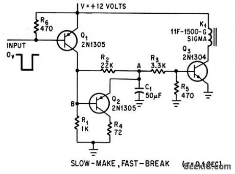
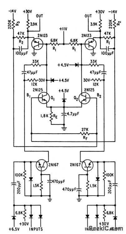
FLIP_FLOP_SPEEDS_MAGNETIC_DETENI_SIEPPING_RELAY
Published:2009/7/14 21:10:00 Author:May
Input signal goes to emitter of saturating flip-flop Q1-Q2, whose condition is sensed by driving transistors Q3-Q4.Stepping coils L1 and L2 are energized according to condition of flip-flop.-F. W. Kear, Coils Operate Stepping Relay at Higher Speed, Electronics, 35:6, p 60-63. (View)
View full Circuit Diagram | Comments | Reading(670)
| Pages:134/471 At 20121122123124125126127128129130131132133134135136137138139140Under 20 |
Circuit Categories
power supply circuit
Amplifier Circuit
Basic Circuit
LED and Light Circuit
Sensor Circuit
Signal Processing
Electrical Equipment Circuit
Control Circuit
Remote Control Circuit
A/D-D/A Converter Circuit
Audio Circuit
Measuring and Test Circuit
Communication Circuit
Computer-Related Circuit
555 Circuit
Automotive Circuit
Repairing Circuit