
Index 133
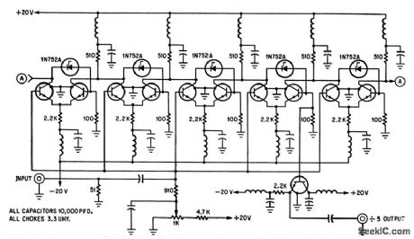
CAPACITOR_BANK_TRIGGER
Published:2009/7/14 21:34:00 Author:May
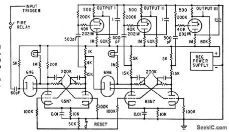
Uses two bistable flip-flops in series as frequency divider for controlling firing of huge capacitor bank. Three outputs deliver pulses with times related to input frequencies.-R. Buser and P. Wolfert, Experimental 100,000 Joule Capcitor Bank for Plasma Research, Electronics,33:32, p 58-61. (View)
View full Circuit Diagram | Comments | Reading(1443)
FSK_DEMODULATOR
Published:2009/7/14 22:36:00 Author:Jessie
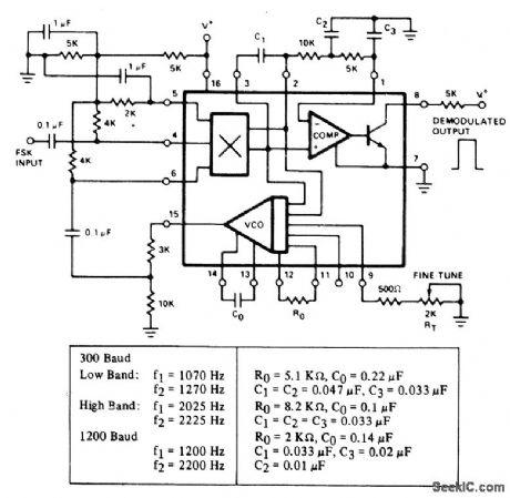
Exar XR-210 FSK modulator-demodulator is connected as PLL system by providing AC coupling between VCO output pin 15 and pin 6. When input frequency isshifted, corresponding to data bit, polarity of DC voltage across phase detector output pins 2 and 3 is reversed. Voltage comparator and logic driver sections convert this DC level shift to binary pulse. C1 serves as PLL filter. C2 and C3 are postdetection filters. Timing capacitor C0 and fine-tune adjustment are used to set VCO midway between mark and space frequencies of input signal. Table gives typical values for 300-baud (103-type) and 1200-baud (202-type) modem applications. Supply can be 5-26 V.- Phase-Locked Loop Data Book, Exar Integrated Systems, Sunnyvale, CA, 1978, p 17-20. (View)
View full Circuit Diagram | Comments | Reading(2724)
SCR_TIME_DELAY
Published:2009/7/14 22:36:00 Author:Jessie
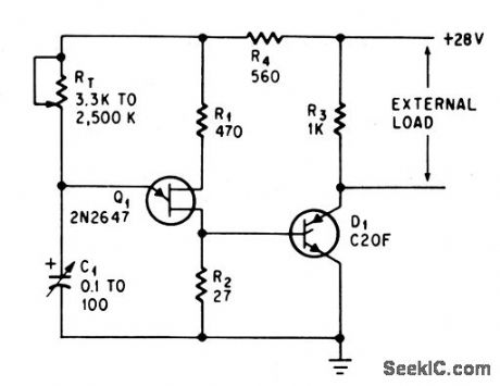
Unijunction transistor Q1 and low-cost scr D1 give time delay of 0.4 millisec to 4 minutes, adjustable by CT-RT.-D. V. Jones, Quick-On-The-Trigger Design, Electronics, 38:12, p 105-110. (View)
View full Circuit Diagram | Comments | Reading(1088)
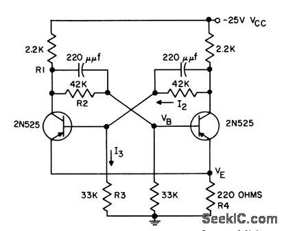
AC_GENERATOR_CUTOUT
Published:2009/7/14 22:35:00 Author:Jessie
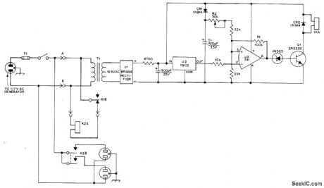
Disconnects equipment from gas-engine generator when AC output exceeds 125-VAC limit determined by setting of R2. Normal 117-VAC output of generator is applied to 12.6-V filament transformer T1. U1 and U2 rectify and regulate one input to comparator U3. CR1 and C1 form peak line-voltage monitor. When pin 3 of U3 exceeds 5 V of pin 2, output of U3 goes positive and turns on al, which applies power to small 12-VDC relay K1. Normally closed contacts of K1 open, removing power from 115-VAC relay K2. 1N523 zener reduces output of U3 enough so Q1 can be turned off. R1 prevents relays from chattering when AC line voltage is close to threshold. To adjust, apply 125 VAC between A and B, and set R2 so K2 drops out.-P. Hansen, Overvoltage Cutout for Field Day Generators, QST, Match 1977, p 49. (View)
View full Circuit Diagram | Comments | Reading(1191)
STABILIZED_MONO
Published:2009/7/14 21:33:00 Author:May
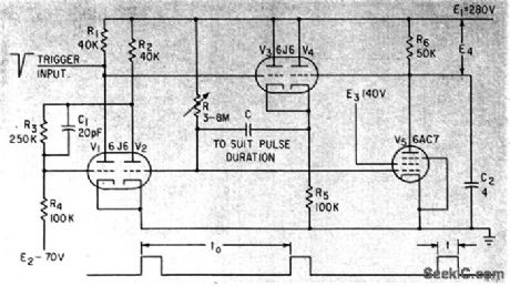
Operates us 10:1 divider at 1,000 pps. Division ratio of mvbr remains constant for supply variations of from 40 to 400 v. Average plate voltage of V5 is adjusted automatically to maintain optimum working conditions throughout operating range.-T. Hornak, Stabilizing Monostable Multivibrators, Electronics, 33:45, p 76. (View)
View full Circuit Diagram | Comments | Reading(749)
RELAY_DELAY
Published:2009/7/14 22:33:00 Author:Jessie
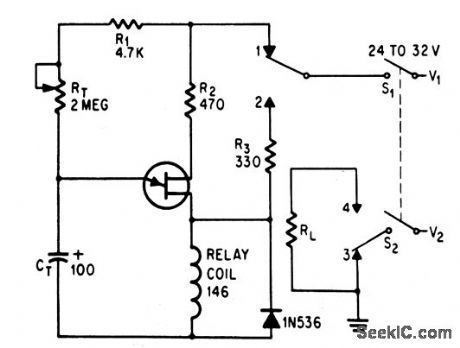
Uuijunction transistor is used to delay operation of relay from 0.5 sec to 3 minutes. CT-RT determine delay interval.-D. V. Jones, Quick-On-The-Trigger Design, Electronics, 38:12, p 105-110. (View)
View full Circuit Diagram | Comments | Reading(871)
VCO_SENSES_VOLTAGE_LIMITS
Published:2009/7/14 21:30:00 Author:May
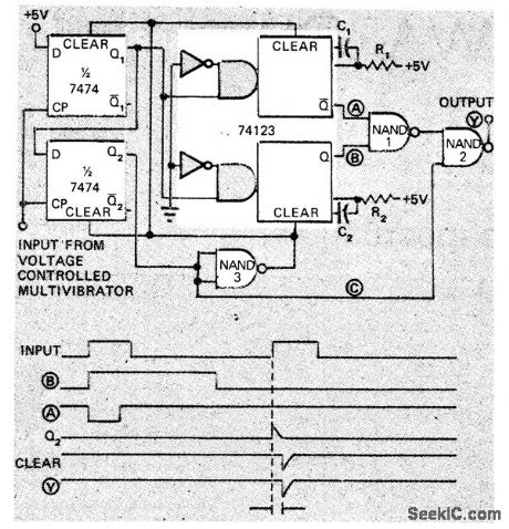
Used to indicate when pulse voltage goes outside preset limits for pulse period. Output pulse rate of voltage-controlled MVBR is monitored to implement double-ended limit detector consisting of 2-bit shift register, two monos, inverter, and two NAND gates. Circuit compares period of input pulses to preset maximum and minimum limits. Output at Y goes low whenever input pulse rate is outside limits, which are deter-mined by R1C1 and R2C2 time constants.-B. Brandstedt, Double-Ended Limit Detector Senses Voltage with VCO, EDN Magazine, Nov. 15, 1972, p 47-48. (View)
View full Circuit Diagram | Comments | Reading(975)
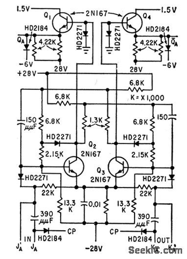
DIVIDE_BY_5_RING_COUNTER
Published:2009/7/14 21:28:00 Author:May
Each stage acts as nonsaturating current-mode switch. Two identical counters are cascaded in uhf prescaler of frequency synthesizer for military uhf transceiver .-L. F. Blachowicz , Dial any Channel to 500 Mhz, Electronics, 39:9, p 60-69. (View)
View full Circuit Diagram | Comments | Reading(1056)
SCALE_OF_TEN_DIVIDER
Published:2009/7/14 21:27:00 Author:May
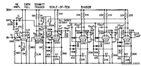
Consists of four cascaded Eccles-Jordan binary dividers with feedback loops, to recycle at 10. Operates up to 500 kc.-J. K. Goodwin, Digital Tachometer Aids in Turbine Design, Electronics, 32:15, p 58-61. (View)
View full Circuit Diagram | Comments | Reading(1118)
FOUR_NUMBER_CALLER
Published:2009/7/14 21:26:00 Author:May
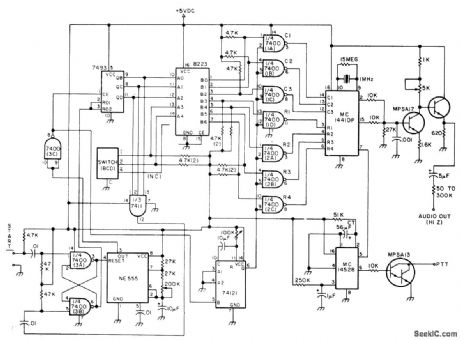
Motorola MC14410 CMOS Touch-Tone generator chip forms basis for automatic dialer using BCD thumbwheel switch to choose telephone number desired.Numbers are stored in 256-bit PR0M by conventional programming. Article shows how auto patch access and disconnect switches are added. To make telephone call from car through repeater, select number desired, push access button and, when dial tone is heard, push start button to transmit tones corresponding to de-sired number. Article covers circuit operation, programming, and coding, and gives additional circuit using 512-bit PR0M to provide eight telephone numbers.-W. J. Hosking, Drive More Safely with a Mobile Dialer, 73 Magazine, Feb. 1977, p 102-104. (View)
View full Circuit Diagram | Comments | Reading(1871)
JK_FLIP_FLOP
Published:2009/7/14 21:26:00 Author:May
Consists of transistorized Eccles-Jordan switch, with collectors damped with diodes to stabilize operating points. Used to provide current for driving gating circuits of voltage amplifiers for magnetic memory drum.-A. J. Strassman and R. E. Keeter, Clock Track Recorder For Memory Drum, Electronics, 32:41, p 74-76. (View)
View full Circuit Diagram | Comments | Reading(913)
SIX_STEP_RING_DELAY
Published:2009/7/14 22:44:00 Author:Jessie
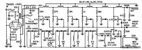
When double-triode blocking oscillator is fired by input trigger, it delivers 0.6-microsec pulse into 1-microsec delay line which, in turn, delivers pulse to next delay line. After sixth delay, pulse is used as trigger for next ring unit.-M. T. Nadir, Microsecond Sampler Handles 126 Channels, Electronics, 32:4, p 36-39. (View)
View full Circuit Diagram | Comments | Reading(1325)
LOW_COST_DISCRIMINATOR
Published:2009/7/14 22:41:00 Author:Jessie


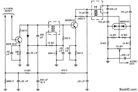
Uses two detectors fed 90° out of phase. Signals are demodulated conventionally for each phase, and the sum of the two signals is token across the whole output. Provides excellent operation as discriminator in 4.5.Mc tv sound detector.-J. B. Compton, A Low-Cost All Solid-Stale FM Discriminator for Consumer Applications, Motorola Application Note AN-212, Jan. 1966.
(View)
View full Circuit Diagram | Comments | Reading(913)
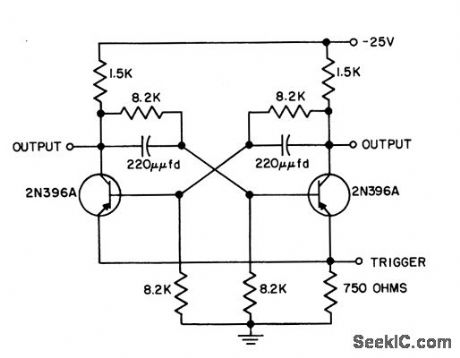
SATURATED_FLIP_FLOP
Published:2009/7/14 21:24:00 Author:May
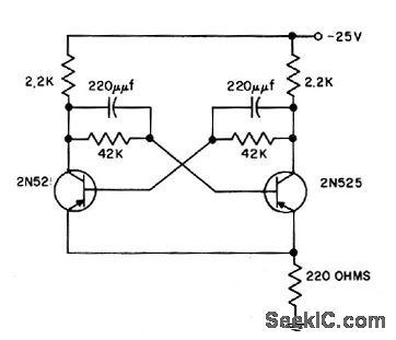
Simple circuit shown is preferable at moderate operating temperatures. If emitter triggering is not used, 220-ohm emitter resistor can be removed.- Transistor Manual, Seventh Edition, General Electric Co., 1964, p 186. (View)
View full Circuit Diagram | Comments | Reading(744)
TWO_TONE_ENCODER
Published:2009/7/14 21:23:00 Author:May
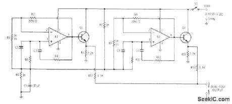
741 opamps and 2N2924 transistors are connected as single-tone encoders producing different audio frequencies、with outputs connected together For2000-Hz tone, use 0.01 μF for c1 and c2 and use 8K for R3 and R4. Formula for frequency of each encoder is f = 0.159/RC where f is in hertz, R in megohms, and C in microfarads; R = R3 = R4 and C = C1 = C2. Frequencies can be chosen for Touch-Tone signaling.-C. D. Rakes, integrated Circuit Projects, Howard W. Sams, Indianapolis, IN, 1975, p 95-97, (View)
View full Circuit Diagram | Comments | Reading(1676)
DCTL_FLIP_FLOP
Published:2009/7/14 21:23:00 Author:May
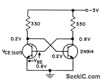
Direct-coupled transistor logic flip-flop utilizes saturation in circuit with extreme simplicity. With silicon transistors, operation up to 150℃ is feasible. Saturation causes storage time delay that limits circuit speed. With germanium transistors, stray voltage signals of about 0.3 v can cause faulty performance.- Transistor Manual, Seventh Edition, General Electric Co., 1964, p 204. (View)
View full Circuit Diagram | Comments | Reading(2359)
SATURATED_FLIP_FLOP_FOR_50℃_
Published:2009/7/14 21:23:00 Author:May
Addition of two 33,000-ohm resistors to basic saturated flip-flop boosts temperature range for stable operation above 50℃.- Transistor Manual, Seventh Edition, General Electric Co., 1964, p 186. (View)
View full Circuit Diagram | Comments | Reading(600)
SINGLE_SCS_FLIP_FLOP
Published:2009/7/14 21:22:00 Author:May
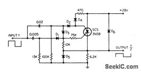
Uses only one silicon controlled switch to perform flip-flop function over wide temperature range. Differentiated positive pulses are applied to cathode pate and anode gate alternately to turn scs on and off. If gate leads are brought out separately, circuit can be used as set-reset flip-flop.-E. Koda, Single-SCS Flip-Flop, EEE, 13;2, p 63. (View)
View full Circuit Diagram | Comments | Reading(788)
SATURATED_FLIP_FLOP_FOR_100℃_
Published:2009/7/14 21:21:00 Author:May
Increased temperature range is obtained at penalty of smaller voltage change at collector, more battery power consumed, and more trigger power required. Capacitor values depend on trigger characteristics and maximum trigger repetition rate.- Transistor Manual, Seventh Edition, General Electric Co., 1964, p 186. (View)
View full Circuit Diagram | Comments | Reading(644)
4_8_V_WINDOW
Published:2009/7/14 21:21:00 Author:May
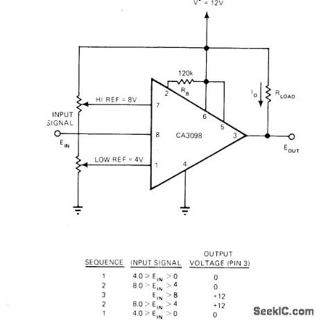
CA3098 dual-input precision level detector tells if data input signal is above or below preset levels of 4 and 8 V. Table gives output states for various input levels. Output current can be up to 150 mA.-G. J. Granieri, Precision Level Detector IC Simplifies Control Circuit Design, EDN Magazine, Oct. 5, 1975, p 69-72. (View)
View full Circuit Diagram | Comments | Reading(638)
| Pages:133/471 At 20121122123124125126127128129130131132133134135136137138139140Under 20 |
Circuit Categories
power supply circuit
Amplifier Circuit
Basic Circuit
LED and Light Circuit
Sensor Circuit
Signal Processing
Electrical Equipment Circuit
Control Circuit
Remote Control Circuit
A/D-D/A Converter Circuit
Audio Circuit
Measuring and Test Circuit
Communication Circuit
Computer-Related Circuit
555 Circuit
Automotive Circuit
Repairing Circuit