
Index 137
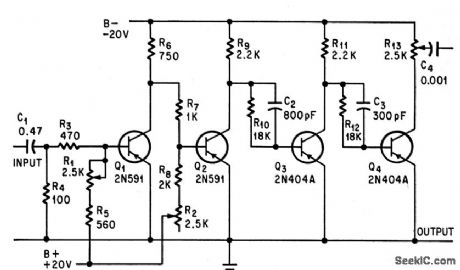
PREFERRED_FAST_RECOVERY_PHANTASTRON_DELAY
Published:2009/7/14 23:26:00 Author:Jessie
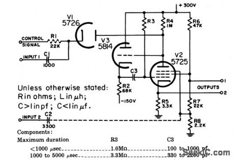


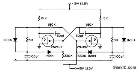
Generates rectangular waveform whose duration is almost directly proportional to control signal. Used to produce movable markers on radar display and to time-modulate pulse in accordance with variable quantities such as antenna position. Maximum recovery time is 40microsec. Control signal is 20 to 240V .input 1 is -15V,and input 2 is -10V.-NBS. Handbook Preferred Circuits Navy Aeronautical Electronic Equipment. Vol.1,Electron Tube Circuits,1963,PC 57,p57-2. (View)
View full Circuit Diagram | Comments | Reading(674)
FSK_GENERATOR_1
Published:2009/7/14 23:23:00 Author:Jessie
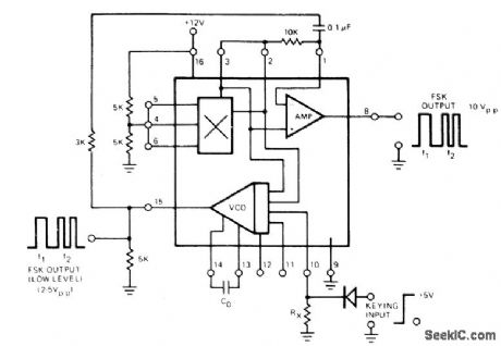
Digital programming capability of Exar XR-215 PLL IC is used to provide shifting of VCO frequency between mark and space frequencies by applying logic pulse to pin 10. Circuit gives 2.5 V P-P output at pin 15 and 1O V P-P output at pin 8, Each output is symmetrical square wave with second harmonic content less than 0.3%. - Phase-Locked Loop Data Book. Exar Integrated Systems, Sunnyvale, CA, 1978, p 21-28. (View)
View full Circuit Diagram | Comments | Reading(886)
SIMPLE_SIGNAL_GENERATOR
Published:2009/7/14 23:19:00 Author:Jessie
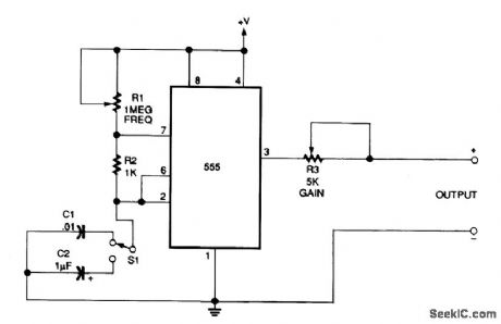
The use of an NE555 allows generation of signals from 1 Hz to higher than 10 kHz. The output is a square wave. (View)
View full Circuit Diagram | Comments | Reading(1571)
555_RAMP_GENERATOR
Published:2009/7/14 23:17:00 Author:Jessie
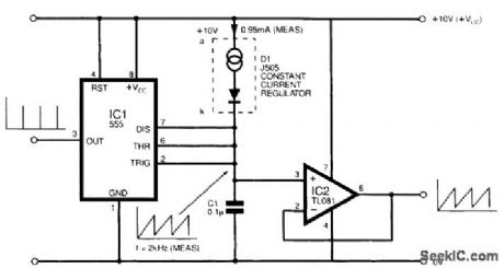
When the timing capacitor of an ordinary 555 circuit charges, an exponential curve across the capacitor results. Obviously, a fast-rising square wave is seen at the output. An accurate ramp voltage can be generated by the 555, though, by ignoring the square-wave output and sneakily using a constant-current source instead of the resistor charging network. The figure shows how a simple J505 constant-current diode can be used to create a reasonable ramp, which will be observed across the capacitor C1. D1 is specified at 1 mA nominal. Assuming that C1 is discharged initially, after power-up the 555 triggers (Vtring, <1/3 Vcc), and C1 starts to charge at a fixed rate through the constant-current source D1 until the threshold voltage of 2/3 Vcc is reached. Then the 555 (IC1) will rapidly discharge the capacitor into pin 7 down to1/3Vcc, when the chip will trigger again. With a 12-V rail, the result is a sawtooth waveform of 4 V p-p. A fast series of spikes is seen at pin 3. (View)
View full Circuit Diagram | Comments | Reading(2356)
BASIC_FET_FLIP_FLOP
Published:2009/7/14 20:47:00 Author:May
Connected as scale-of-two binary frequency divider, complete with steering diodes, speedup capacitors, and coupling capacitors. Used where speed is not primary consideration.-L. J. Sevin , Jr., Field-Effect Transistors, McGraw-Hill, N.Y., 1965, p 89. (View)
View full Circuit Diagram | Comments | Reading(1449)
BANDPASS_FOR_170_Hz_RIIY_SHlFI
Published:2009/7/14 23:17:00 Author:Jessie
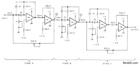
Three-stage active Butterworth bandpass input filter is used in radioteletype demodulator to separate RTTY tones from each other and from noise. Filter is centered on 2200 Hz, and has bandpass of about 260 Hz to allow reception of some of audio sidebands produced by keying and allow for small drift. Five pots serve for trimming center frequency of each stage andQ of end stages. Article gives step-by-step design and alignment procedures. Use two 10K resistors between V and ground to get V/2 for bias when operating from single supply.-P. A. Stark, Design an Active RTTY Filter, 73 Magazine, Sept. 1977, p 38-43.
(View)
View full Circuit Diagram | Comments | Reading(1197)
BINARY_FLIP_FLOP_IURNS_ON
Published:2009/7/14 20:47:00 Author:May
Triggering is accomplished by turning transistors on, whereas in most similar circuits the transistors are turned off. Trigger pulse merely has to lower point o below ground for fraction of microsecond. Almost any diode and transistor can be used. Speed can be up to 10 Mc with high-speed transistors. Output fall time is fast.-Binary Flip-Flop Tums On, Electronic Circuit Design Handbook, Mactier Pub. Corp., N.Y., 1965, p 214. (View)
View full Circuit Diagram | Comments | Reading(707)
FSK_DECODER
Published:2009/7/14 23:11:00 Author:Jessie
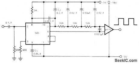
Simple circuit for Signetics NE565 PLL locks to input frequency and tracks it between two values used, to produce corresponding DC shift at output. Values shown are for 1070-Hz and 1270-Hz FSK signals. Three-stage RC ladder filter removes sum frequency component. Band edge of filter is chosen to be about halfway between maximum keying rate (150 Hz) and twice input frequency (about 2200 Hz). Output is made logic-compatible by connecting voltage comparator to pin 6.- Signetics Analog Data Manual, Signetics, Sunnyvale, CA, 1977, p 845. (View)
View full Circuit Diagram | Comments | Reading(1958)
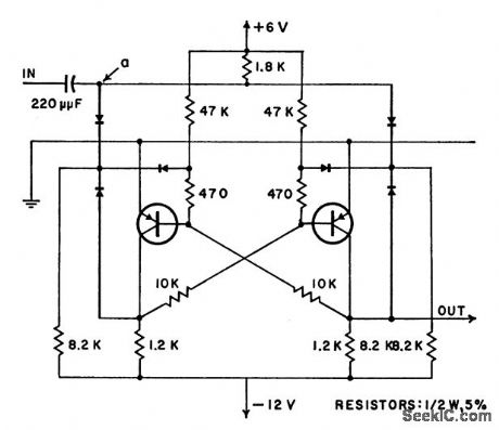
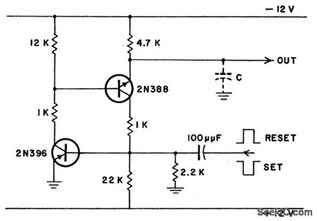
PAIRED_INVERTERS
Published:2009/7/14 20:46:00 Author:May
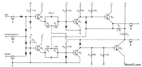
Cross-coupling of two basic inverters gives low-cost lip-lop using 2N711 germanium pnp mesa switching transistors. Flip-flop can be set and then reset, or run as Gaunter using combined input. Close regulation is required for -4 v supply.-P. A. Mclnnis, Low-Cost Computer Circuits, Motorola Application Note AN-130, Nov. 1965. (View)
View full Circuit Diagram | Comments | Reading(673)
AC_OVERVOLTAGE
Published:2009/7/14 23:09:00 Author:Jessie
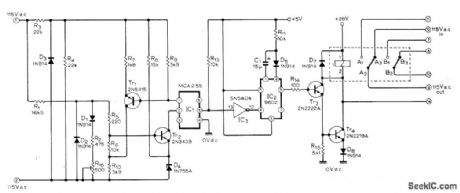
Used to protect delicate equipment from sustained high AC line voltage, by disconnecting supply when it exceeds preset level selected by R16. When base-emitter voltage of Tr2 exceeds 7.5 V, optocoupler switches Tr1 on to provide fast switching action. Output pulse is shaped by IC3 for use in triggering mono IC2. When line falls below preset level, mono reverts to stable state and switches on AC supply again.-F. E. George, A.C. Line Sensor, Wireless World, March 1977, p 42. (View)
View full Circuit Diagram | Comments | Reading(878)
PLL_TOUCH_TONE_DECODER
Published:2009/7/14 20:45:00 Author:May
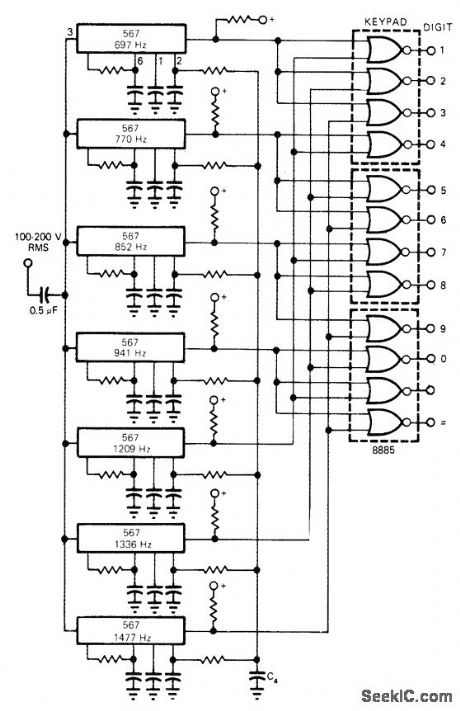
Seven 567 PLLs sense presence of selected tones from common 100-200 VBMS input line, while 8885 NOR gates perform necessary decoding logic to generate decimal outputs. Circuit takes advantage of good frequency selectivity provided by lock-and-capture ranges of PLLs, as required for discriminating against many tones.-E. Murthi, Monolithic Phase-Locked Loops-Analogs Do All the Work of Digitals, and Much More, EDN Magazine, Sept. 5, 1977, p 59-64. (View)
View full Circuit Diagram | Comments | Reading(754)
ZERO_CROSSING_DETECTOR
Published:2009/7/14 23:07:00 Author:Jessie
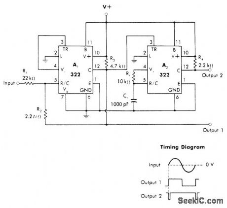
Output 1 of 322 comparator A1 is high when input signal is above zero and low when input is below zero. Output of comparator A1 is thus square wave in phase with zero crossings of input. When R1, is 22K, input can be up to ±10 V amplitude. A2 is mono MVBR connected to fire when output 1 of A1 goes high (at zero crossings). Resulting negative-going narrow pulses at output 2 are useful for time marks.-W. G. Jung, IC Timer Cook-book, Howard W. Sams, Indianapolis, IN, 1977, p 152. (View)
View full Circuit Diagram | Comments | Reading(3189)
NONSTALLING_FLIP_FLOP_FOR_CAPACITIVE_LOAD
Published:2009/7/14 20:44:00 Author:May
Used for transferring data into storage having heavy capacitive load, such as long connecting wires. Complementary con figuration, with load in emitter circuit of one transistor, makes stage trigger reliably in fraction of microsecond.-Non-Stalling Flip-Flop for Capacitive Load, Electronic Circuit Design Handbook, Mactier Pub. Corp., N.Y., 1965, p 213. (View)
View full Circuit Diagram | Comments | Reading(770)
SIMPLE_VCO_DRIVER
Published:2009/7/14 20:43:00 Author:May
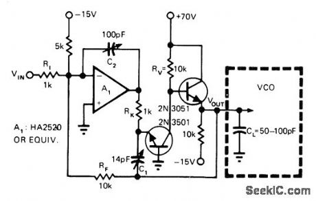
Provides full output of 60 V P-P up to 1 MHz Slew rate is 200 V/μs, and small-signal bandwidth is 5 MHz. Uses fastinput opamp, voltage buffer, and simple compensation technique. C2 is trimmed for stability, while C1 is adjusted to increase slew rate and bandwidth. -H Bunin, Low Cost VCO Driver Amplifiers Really Perform If Designed Right, EDN Magazine, Oct 5. 1974, p 51-55. (View)
View full Circuit Diagram | Comments | Reading(1110)
WINDOW_DETECTOR_1
Published:2009/7/14 23:05:00 Author:Jessie
Unique voltage-range sensing circuit provides positive indications of high, low or acceptable input levels for voltage and includes adjustments for both threshold and hysteresis levels. R1 and R2 ad just upper and lower thresholds, while R3 and R4 adjust upper and lower hysteresis levels. If acceptable input range is 4.5 V to 5.5V, output of opamp A1 goes negative when ein is greater than 5.5V. This saturates Q1 and Q2, making Q2 output go from 5 V to 0. TTL then indicates that input has exceeded 5,5 V. Upper hysteresis keeps A1 output negative until input has dropped to setting of R3, which might be 5.3 V. Similarly, when input drops below 4.5 V, output of A2 goes positive and saturates Q3.-I. KrellAnalogMonitor Has Threshold and Hysteresis Controls, EDN Magazine, Aug.1, 1972, p 58. (View)
View full Circuit Diagram | Comments | Reading(1567)
TRANSCEIVER_SAVER
Published:2009/7/14 23:05:00 Author:Jessie
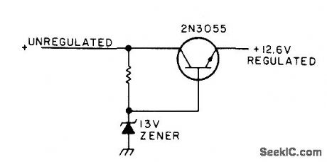
Simple circuit has no effect on normal operation of CB transceiver or other solid-state equipment in auto but provides overvoltage protection if voltage regulator in auto fails. Use heatsink with transistor if transmit current is above 2 A. Choose resistance value to give output of 12.6 V during normal operation.-Circuits, 73 Magazine, March 1977, p 152. (View)
View full Circuit Diagram | Comments | Reading(1431)
058_TO_465_MICROSEC_DELAY
Published:2009/7/14 23:04:00 Author:Jessie
Saturated germanium transistors give variable time delay for 27-V input pulse having 2.75-microsec width, with R2 controlling delay time and R1 controlling output pulse width.-R. H. Blumenthal and F. E. Williams, Transistor's Stored Charge Controls Pulse Delay, Electronics, 37:19, p 52-53. (View)
View full Circuit Diagram | Comments | Reading(1122)
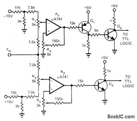
TOUCH_TONE_DECODER
Published:2009/7/14 20:42:00 Author:May
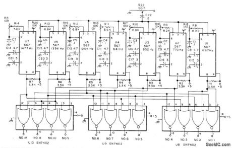
Uses seven National LM567 phase-locked loop decoders (U1-U7) having high noise rejection, immunity to false signals, and stable center frequency. Each 567 activates proper gate of SN7402, making output of gate go to high or 1 state for driving NPN transistor that can turn on LED labeled with corresponding Touch-Tone number. Alternatively, gate outputs can drive 12 relays, with relay contacts going to LEDs and/or to keyboard switches of ordinary calculator used as display display. Article tells how to adjust 10K pot for each 567 for detection of desired frequency.-W. Mac-Dowell, Touch-Tone Decoder, 73 Magazine, June 1976, p 26-27. (View)
View full Circuit Diagram | Comments | Reading(3488)
PLL_FSK_DEMODU_LATOR
Published:2009/7/14 23:04:00 Author:Jessie
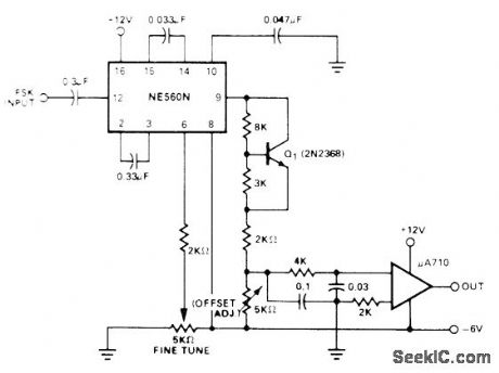
Signetics NE560N phase-locked loop is used as receiving converter for demodulating carrier shifted between two preset frequencies, one corresponding to 0 and other to 1 of binary data signal. PLL provides shifting DC voltage to initiate 1 or 0 (mark or space) code elements. Circuit locks on and tracks output frequency of receiver. Input at pin 12 should be from 30 mV to 2 V P-P square or sine wave. Output of about 60 mVDC at pin 9 is amplified, conditioned, and fed to μA710 comparator to provide proper output voltages for interfacing with printer- Signetics Analog Data Manual, Signetics, Sunnyvale, CA, 1977, p 844-845. (View)
View full Circuit Diagram | Comments | Reading(684)
5_V_CROWBAR
Published:2009/7/14 23:03:00 Author:Jessie
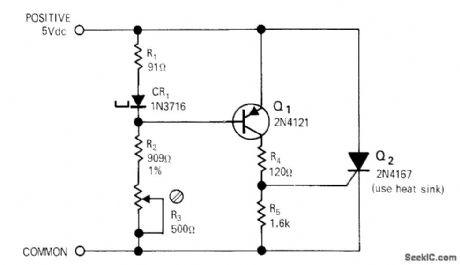
Simple overvoltage protection circuit for 5-V 1-A logic supply can be adjusted to trigger at 10% overvoltage or 5.5 V. Tunnel diode CR1 senses level. At 5.5 V, diode switches slightly past its valley piont, and voltage across diode biases Q1 into saturation. Q1 then supplies gate current to SCR Q2, which fires and continues conducting until power supply is disconnected. Power supply must include current-limiting circuit and fuse. R3 adjusts trip point.-L. Strahan, Logic-Supply Crowbar, EDN|EEE Magazine, Nov. 15, 1971, p 51. (View)
View full Circuit Diagram | Comments | Reading(2456)
| Pages:137/471 At 20121122123124125126127128129130131132133134135136137138139140Under 20 |
Circuit Categories
power supply circuit
Amplifier Circuit
Basic Circuit
LED and Light Circuit
Sensor Circuit
Signal Processing
Electrical Equipment Circuit
Control Circuit
Remote Control Circuit
A/D-D/A Converter Circuit
Audio Circuit
Measuring and Test Circuit
Communication Circuit
Computer-Related Circuit
555 Circuit
Automotive Circuit
Repairing Circuit