
Basic Circuit
Index 351
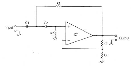
ACTIVE_LOW_PASS_FILTER
Published:2009/6/19 2:04:00 Author:May
This circuit has a rolloff of 6 dB/Octave. (View)
View full Circuit Diagram | Comments | Reading(0)
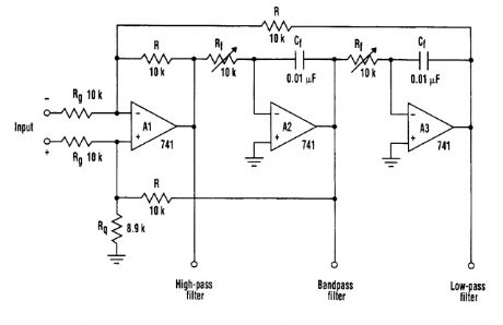
PROGRAMMABLE_ANALOG_FILTER
Published:2009/6/19 2:03:00 Author:May
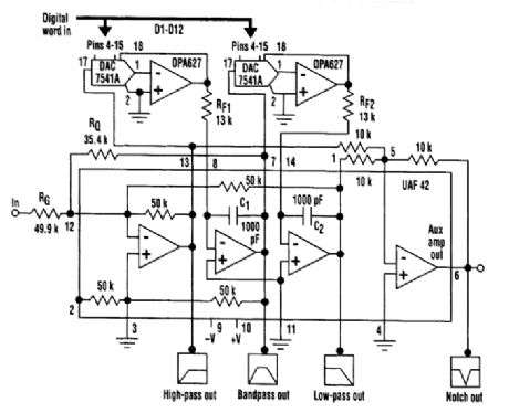
The circuit in the figure shows how an analog, digitally programmable filter can be built using a UAF42. This monolithic, state-variable active filter chip provides a two-pole filter building block with low sensitivity to extemal component variations. It eliminates aliasing errors and clock feed though noise common to switched-capacitor filters. Low-pass, high-pass, bandpass, and notch (band-reject) outputs are available. (View)
View full Circuit Diagram | Comments | Reading(1766)
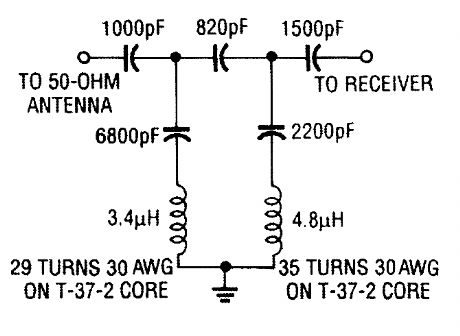
SHORTWAVE_INTERFERENCE_TRAP
Published:2009/6/19 2:01:00 Author:May
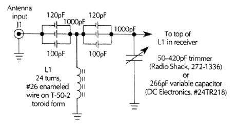
Build this interference trap to help block strong shortwave, broadcast, and FM stations from corning in on the shortwave bands. (View)
View full Circuit Diagram | Comments | Reading(971)
HIGH_PASS_ACTIVE_FILTER
Published:2009/6/19 1:59:00 Author:May
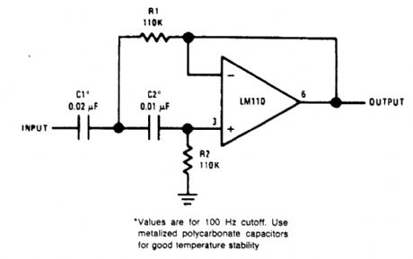
View full Circuit Diagram | Comments | Reading(1)
PIN_DIODE_FILTER_SELECTION_CIRCUIT
Published:2009/6/19 1:59:00 Author:May
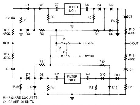
Selecting IF bandpass filters via series/shunt PIN-diode switching can be accomplished with this circuit. (View)
View full Circuit Diagram | Comments | Reading(913)
SHORTWAVE_RECEIVER_IF_FILTER
Published:2009/6/19 1:58:00 Author:May
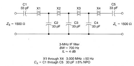
An inexpensive filter can be made from microprocessor crystals. This filter has 700 Hz BW (3 dB) and has a flat response (<1 dB) for about 400 to 500 Hz. Although a 3-MHz crystal was used, any frequency from 2 to 15 MHz (using fundamental crystal) should work, with appropriate scaling of components. Crystal resonant frequencies should match within 20% and preferably 10% of expected bandwidth (which is narrower as Cx increases. Impedance is reduced with wider bandwidths. (View)
View full Circuit Diagram | Comments | Reading(820)
COMBINATION_FILTER
Published:2009/6/19 1:57:00 Author:May
The classic state variable two-integrator filter is known for its insensitivity to component varia-tions, and its ability to provide three separate simultaneous outputs-low pass, high pass, and bandpass.Typically, a quad op amp is used to implement the state-variable filter. The classic configuration uses two integrating amplifiers, a filter input amplifier, and a filter feedback amplifier.The design described here combines both input and feedback amplifiers into one adder/subtrac-tor amplifier, achieving a three op-amp filter design (see the figure). (View)
View full Circuit Diagram | Comments | Reading(1843)
SECOND_ORDER_VOLTAGE_CONTROLLED_FILTER
Published:2009/6/19 1:55:00 Author:May
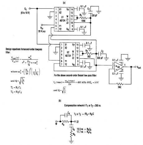
Desirable second-order voltage-controlled low-pass filter response can be achieved with this voltage-controlled filter (A). By using low-distortion, wide-bandwidth multipliers, it achieves higher cutoff frequencies than sv(itched-capacitor filters. If the circuit's RC network has a time constant less than 200 ns, it should be replaced by a lag compensator network (B). (View)
View full Circuit Diagram | Comments | Reading(771)
MINUTE_MARKER
Published:2009/6/19 1:54:00 Author:May
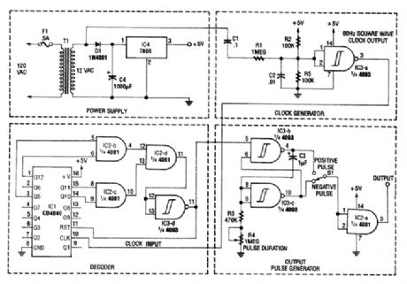
The figure shows the schematic of a minute marker. The output of transformer T1 is 12.6 Vac at 60 Hz, which is rectified by D1 and regulated by IC4, and LM7805 regulator, to provide 5 Vdc for the circuit. The unrectified ac is bandpass-filtered by R1, R2, R5, C1, and C2. Resistors R2 and R5 also form a dcvoltqge divider, which biases the input of Schmitt trigger IC3-a to 2.5 V. The Schrnitt trigger generates a 60-Hz square wave, which is fed to the input of IC1, a CE4040 12stage binary counter.The outputs of the counter are a 4081 quad AND gate (IC2), and the decoded output is fed back to the reset input of the counter, which resets the counter when the desired count is reached.The pulse from IC2-d is inverted by Schmitt trigger IC3-d, and passed along to the output pulse generator. The output pulse is generated by two Schmitt triggers cross-connected as an RS flip-flop (IC3-b and IC3-c). The output of the flip-flop is fed to 3, R4, and C3, whose values set the output pulse duration. The output pulse duration (T) can be approximated by the formula T=1.2×C3×(R3+ R4).A positive or negative-going pulse is selected by 51, and buffered by the remaining AND gate (IC2-a). (View)
View full Circuit Diagram | Comments | Reading(907)
HIGH_PASS_FILTER
Published:2009/6/19 1:54:00 Author:May
This high-pass filter will attenuate AM stations by 40 dB. Its low-frequency cutoff is about 2.2 MHz. This filter is useful for SW listening in areas of high AM radio signal strength. (View)
View full Circuit Diagram | Comments | Reading(1050)
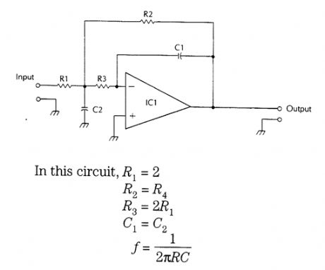
ACTIVE_BANDPASS_FILTER_CIRCUIT
Published:2009/6/19 1:52:00 Author:May
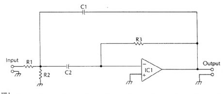
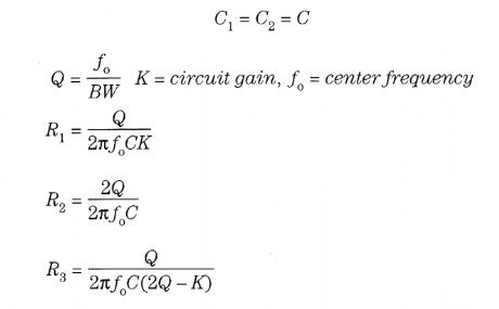
In this circuit, (View)
View full Circuit Diagram | Comments | Reading(728)
SALLEN_KEY_HIGH_PASS_FILTER
Published:2009/6/19 1:50:00 Author:May

R3 and R4 set the circuit galn (View)
View full Circuit Diagram | Comments | Reading(805)
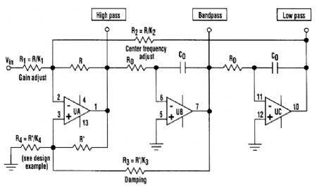
STAET_VARIABLE_FILTER
Published:2009/6/19 1:49:00 Author:May
The state variable filter shown consists of only three op amps and a few passive components. It provides several key features. These include the ability to simultaneously provide low-pass, high-pass, and bandpass filter functions, and adjust bandwidth in a wide range by changing the values of Cf and Rf. The device also is easy to tune and simple to congtruct, while the quality factor (Q) of each filter is independent of each other. (View)
View full Circuit Diagram | Comments | Reading(1011)
SIMPLE_LOCK
Published:2009/6/19 1:44:00 Author:May
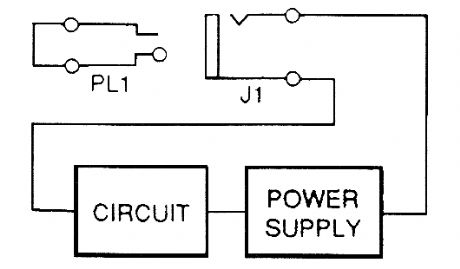
Only an appropriately wired plug of the right size will activate circuits with a nonshorting jack in their power supply circuit. (View)
View full Circuit Diagram | Comments | Reading(793)
FREQUENCY_BASED_LOCK
Published:2009/6/19 1:38:00 Author:May

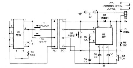


The system is formed by two separate circuits-a key and a keyhole. The key engages the key-hole with a mating pair of connectors. The key is a tone-generator circuit consisting of a 4049 hex in-verter CMOS IC (U1), switches (S1 and S2), a resistor (R1), and a capacitor (C1). The value of the tone generated by that circuit in Hz is determined by;The keyhole is a 567 tone-decoder circuit that can be conftgured to detect any frequency from 0.01 Hz to 500 kHz. The frequency it detects (fo), via the 567 IC, turns on the relay (K1). Compo-nents R3 and D1 are used to latch the circuit, so the output stays on even after the input tone is re-moved. When S2 is pressed, the system is reset. Switch S3 resets the circuit from inside. (View)
View full Circuit Diagram | Comments | Reading(992)
DMAl0 rectification module functional diagram
Published:2011/4/14 1:32:00 Author:muriel | Keyword: rectification module, functional diagram
View full Circuit Diagram | Comments | Reading(455)
ELECTRONIC_LOCK
Published:2009/6/19 1:36:00 Author:May
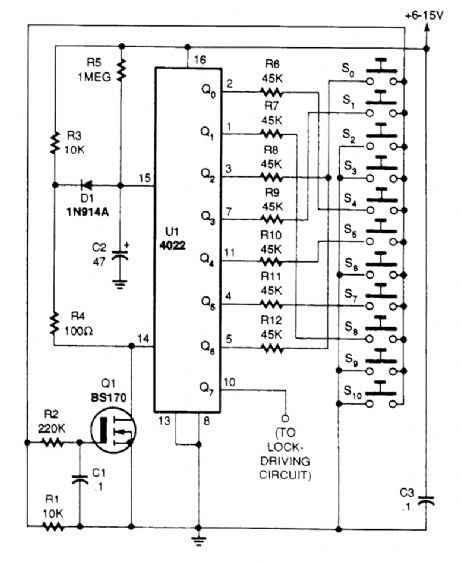
The heart of the circuit is a 4022 octal counter. When first powered up, C2 is charged via R5, so the reset input of the couitter is kept high. That causes output Qo to go high while all other outputs are low. With the switches wired as shown, when 54 is pressed, the BS170 is switched on via de-bouncing network R2/C1, and U1 receives a clock pulse. Also, C2 is discharged via R4 and D1 removing the reset signal of the counter, allowing it to advance. The time required for C2 to charge via R5 (e.g., to reset the counter), is the maximum time that can lapse before the next key is pressed.The above cycle is therefore repeated only if S8 (connected to the Q1 output) is pressed in time.When all keys have been pressed in time and in the correct order, Q7 goes high for about four sec-onds to drive the unlock circuitry (e.g., a relay driver for an automatic door opener. A builder can change the code by reviewing the switches. The code for the lock shown in the circuit diagram is 4-8-0-1-5-7-0. However, the 4022 octal counter can be replaced by a 4017 divide-by-10 counter. That will make it possible to add two more digits to the combination. (View)
View full Circuit Diagram | Comments | Reading(4)
BIPOLAR_STEPPER_MOTOR_DRIVE_CIRCUIT
Published:2009/6/18 23:39:00 Author:May
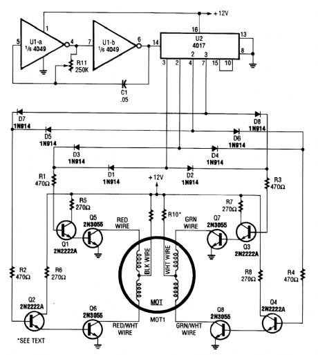
A 4017 decade counter/divider driven from a low-frequency oscillator (U1-a and U1-b) is used to drive transistor switches to sequence the windings, as is needed. MOT1 is a 12-V stepper motor. R9 and R10 are selected for the motor's current rating. A 3.3-Hz signal from UI will cause the motor to run at 1 rpm, a 33-Hz signal will result in 10 rum, etc. (View)
View full Circuit Diagram | Comments | Reading(2300)
VARIABLE_VOLTAGE_ATTENUATOR
Published:2009/6/18 23:28:00 Author:May
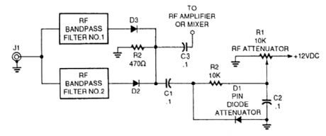
The front-end of this circuit is a bank of selectable bandpass filters. The output of the filter banks are shunted to ground via capacitor (C1) and PIN diode (D1). The PIN diode acts like an electroni-cally variable resistor. The resistance across the diode's terminals is a function of the applied bias voltage. This voltage, hence the degree of attenuation of the RE signal, is proportional to the setting of potentiometer RI. The series resistor (R2) is used to limit the current when the diode is forward biased. This step is necessary because the diode has a very low resistance when a certain rather low potential is exceeded. (View)
View full Circuit Diagram | Comments | Reading(858)
SWITCHABLE_POWER_ATTENUATOR
Published:2009/6/18 23:27:00 Author:May
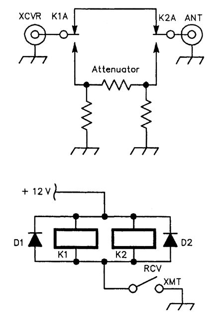
Schematic diagram of a switchable power attenuator that can be used to reduce the power output of transmitters that don't have ALC lines.
Values for 10 and 20 dB: 10 dB: R1 = R3 = 91 ΩR2 = 75 Ωnearest standard values 20 dB: R1 = R3 = 62Ω R2= 240 Ω nearest standard values
Note: R1 must handle the largest share of the input power, and R2 somewhat less. This depends on attenuation selected. (View)
View full Circuit Diagram | Comments | Reading(665)
| Pages:351/471 At 20341342343344345346347348349350351352353354355356357358359360Under 20 |
Circuit Categories
power supply circuit
Amplifier Circuit
Basic Circuit
LED and Light Circuit
Sensor Circuit
Signal Processing
Electrical Equipment Circuit
Control Circuit
Remote Control Circuit
A/D-D/A Converter Circuit
Audio Circuit
Measuring and Test Circuit
Communication Circuit
Computer-Related Circuit
555 Circuit
Automotive Circuit
Repairing Circuit