
Basic Circuit
Index 357
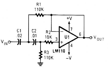
ACTIVE_LOW_PASS_RC_FILTER
Published:2009/6/16 2:32:00 Author:May
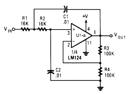
The circuit shown has a cutoff frequency at about 1 kHz. R1, R2, C1, and C2 can be scaled to change this to any other desired frequency. (View)
View full Circuit Diagram | Comments | Reading(1007)
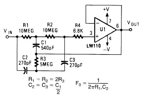
BANDPASS_FILTER_1
Published:2009/6/16 2:32:00 Author:May
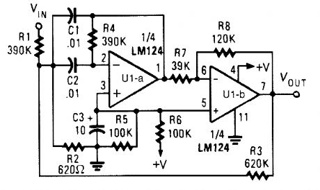
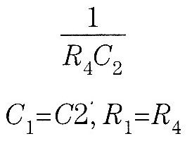
Appropriate center frequency of this circuit is:
(View)
View full Circuit Diagram | Comments | Reading(694)
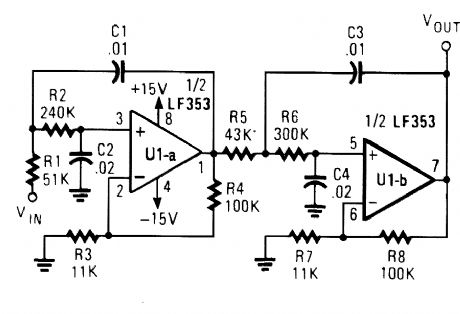
400_Hz_LOW_PASS_BUTTERWORTH_FILTER
Published:2009/6/16 2:30:00 Author:May
Designed for a 400-Hz cutoff frequency, the cutoff can be scaled by varying the element values proportionally to frequency (View)
View full Circuit Diagram | Comments | Reading(791)
ACTIVE_HIGH_PASS_FILTER
Published:2009/6/16 2:27:00 Author:May
View full Circuit Diagram | Comments | Reading(951)
FOURTH_ORDER_LOW_PASS_BUTTERWORTH_FILTER
Published:2009/6/16 2:27:00 Author:May
View full Circuit Diagram | Comments | Reading(914)
BANDPASS_FILTER
Published:2009/6/16 2:26:00 Author:May
View full Circuit Diagram | Comments | Reading(111)
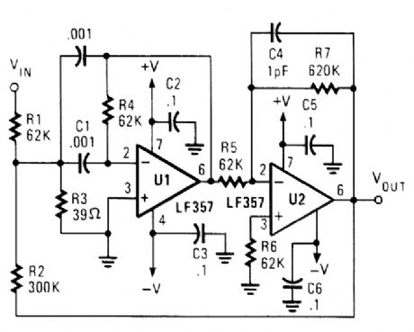
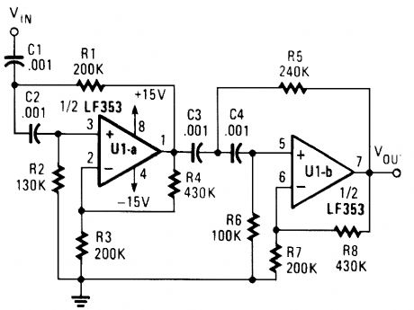
HIGH_Q_BANDPASS_FILTER
Published:2009/6/16 2:24:00 Author:May
View full Circuit Diagram | Comments | Reading(1927)
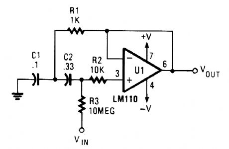
TUNABLE_NOTCH_FILTER
Published:2009/6/16 2:23:00 Author:May
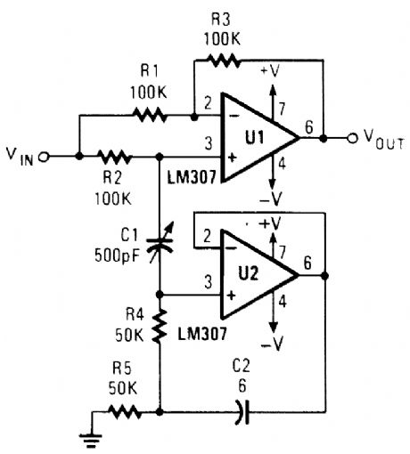
View full Circuit Diagram | Comments | Reading(1201)
FOURTH_ORDER_HIGH_PASS_BUTTERWORTH_FILTER
Published:2009/6/16 2:22:00 Author:May
View full Circuit Diagram | Comments | Reading(974)
ADJUSTABLE_Q_NOTCH_FILTER
Published:2009/6/16 2:21:00 Author:May
View full Circuit Diagram | Comments | Reading(2)
UNIVERSAL_STALE_VARIABLE_FILTER
Published:2009/6/16 2:19:00 Author:May
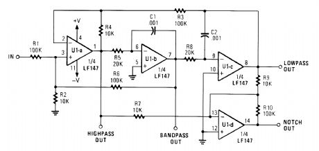
View full Circuit Diagram | Comments | Reading(665)
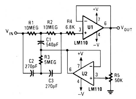
HIGH_Q_NOTCH_FILTER
Published:2009/6/16 2:18:00 Author:May
View full Circuit Diagram | Comments | Reading(1)
ACTIVE_LOW_PASS_FILTER
Published:2009/6/16 2:18:00 Author:May
View full Circuit Diagram | Comments | Reading(814)
10_TO_1_Hz_TIMEBASE
Published:2009/6/15 21:16:00 Author:May
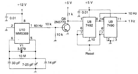
This system uses an MM5369 IC to derive a 60-Hz signal from a TV burst crystal (3579 MHz). V8 and V9 produce a 10-Hz and 1-Hz signal from this 60-Hz signal. Y1 can be any parallel-mode 3.579-MHz crystal. (View)
View full Circuit Diagram | Comments | Reading(1626)
CRYSTAL_ACTIVITY_TESTER
Published:2009/6/15 21:15:00 Author:May
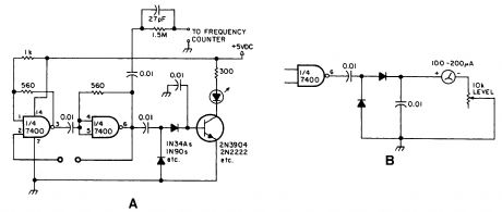
This circuit will check a crystal for activity.Two sections of a 7400 act as an oscillator and its out-put is rectified and drives an npn transistor that switches an LED (Fig.A).In Fig.B, a meter replaces the LED. (View)
View full Circuit Diagram | Comments | Reading(2)
MULTI_OUTPUT_TIMEBASE
Published:2009/6/15 21:12:00 Author:May
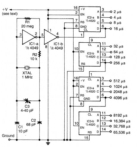
A 1-MHz oscillator drives a binary counter to produce pulse widths from 2 to 65,536 ms. V+ is any CMOS suitable level (5 to 15 V, etc.). (View)
View full Circuit Diagram | Comments | Reading(2098)
LOW_FREQUENCY_CRYSTAL_OSCILLATOR
Published:2009/6/15 20:55:00 Author:May
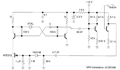
Q1, Q2, and the associated circuitry form a modified astable multivibrator in which the loop gain is automatically adjusted to the threshold of oscillation by means of field effect transistor Q3. Q4 lin-early amplifies the signal present at the collector of Q2 and isolates the oscillator section of the cir-cuit from the output. This stage features wideband operation and delivers a clean 2.5-V amplitude sine wave into a resistive load greater than or equal to 20 kΩ. The stage comprising Q5 has a voltage gain of 1 and its sole purpose is to isolate the nonlinear effects of rectifier Dl from the output. (View)
View full Circuit Diagram | Comments | Reading(2021)
DUAL_BAND_LOOP_ANTENNA_FOR_80__160_m
Published:2009/6/15 20:48:00 Author:May
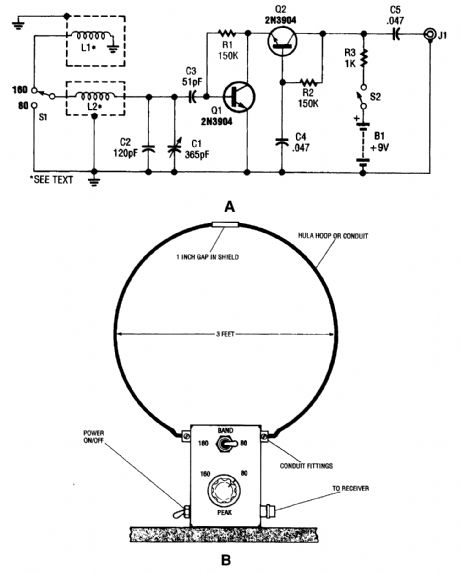
This antenna might help to reduce power-line noise. A plastic hula hoop or conduit 3 feet in diameter, covered with aluminum foil as a shield is used for L1 and L2. L1 is two turns and L2 is one turn, threaded through the loop. S1 selects 160- or 80-m operation. Q1 and Q2 form a preamplifier for the loop antenna. Do not transmit with this antenna-it is for receiving only. (View)
View full Circuit Diagram | Comments | Reading(2553)
2_MHz_FREQUENCY_COUNTER
Published:2009/6/15 20:48:00 Author:May
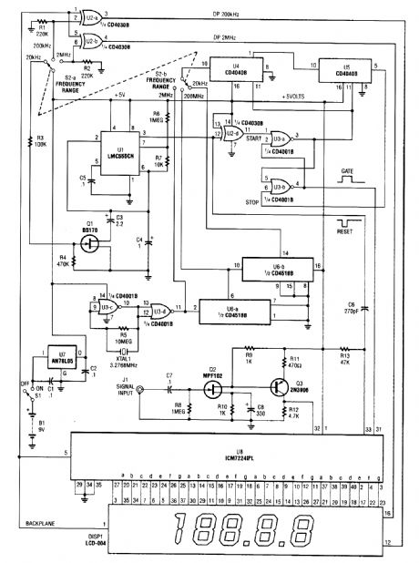

This is a schematic and block diagram of a 2-MHz frequency counter. It uses and LSI counter/display driver, LCD readout, and a,few logic chips for timebase and timing pulse circuitry. Q2 and Q3 form a signal (input) amplifier.The circuit contains a crystal oscillator built around U3-c and XTALl, which provides the pri-mary timing-reference signal. That signal is then divided twice to provide two additional timing ref-erences, giving the circuitry three selectable timing references. The ICM7224IPL is an integrated circuit that consists of the counter and display driver to drive the LCD-004 display. (View)
View full Circuit Diagram | Comments | Reading(3582)
LEAD_ACID_BATTERY_CHARGER
Published:2009/7/6 4:27:00 Author:jailer
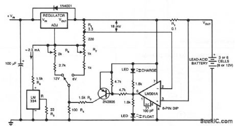
This circuit furnishes an initial voltage of 2.5 V per cell at 25℃ to rapidly charge a battery. The charging current decreases as the battery charges, and when the current drops to 180 mA, the charging circuit reduces the output voltage to 2.35 V per cell, leaving the battery in a fully charged state. This lower voltage prevents the battery from overcharging, which would shorten its life.
The LM301A compares the voltage drop across R1 with an 18 mV reference set by R2. The comparator's output controls the voltage regulator, forcing it to produce the lower float voltage when the battery-charging current, passing through R1, drops below 180 mA. The 150 mV difference between the charge and float voltages is set by the ratio of R3 to R4. The LEDs show the state of the circuit.
Temperature compensation helps prevent overcharging, particularly when a battery undergoes wide temperature changes while being charged. The LM334 temperature sensor should be placed near or on the battery to decrease the charging voltage by 4 mV/℃ for each cell. Because batteries need more temperature compensation at lower temperatures, change R5 to 30 Ωfor a tc of -5 mV/℃ per cell if application will see temperatures below -20℃.
The charger's input voltage must be filtered dc that is at least 3 V higher than the maximum required output voltage: approximately 2.5 V per cell. Choose a regulator for the maximum current needed: LM371 for 2 A, LM350 for 4 A, or LM338 for 8 A. At 25℃ and with no output load, adjust R7 for a VOUT of 7.05 V, and adjust R8 for a VOUT of 14.1V. (View)
View full Circuit Diagram | Comments | Reading(3789)
| Pages:357/471 At 20341342343344345346347348349350351352353354355356357358359360Under 20 |
Circuit Categories
power supply circuit
Amplifier Circuit
Basic Circuit
LED and Light Circuit
Sensor Circuit
Signal Processing
Electrical Equipment Circuit
Control Circuit
Remote Control Circuit
A/D-D/A Converter Circuit
Audio Circuit
Measuring and Test Circuit
Communication Circuit
Computer-Related Circuit
555 Circuit
Automotive Circuit
Repairing Circuit