
Basic Circuit
Index 347
SUPPRESS_JITTER_WITH_HYSTERESIS
Published:2009/6/22 22:40:00 Author:May
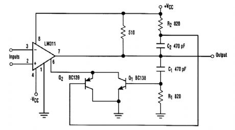
When the comparator's output changes its state from low to high, the rising edge of the output pulse, differentiated by the C1/R1 chain, opens Q1. This blocks comparator M via its strobing input and sustains its output in the H state for a period of time, defined by the time constant R,Ct After C1 is charged by the current flowing through R1, Q1 is shut off and the comparator is released. When the comparator's output state changes from high to low, a similar process, involving elements R2, C2, and Q2, occurs. In many applications, the output transition in only one direction is of vital importance, and the elements, which provide temporal hysteresis for the opposite direction transition, can be omitted. (View)
View full Circuit Diagram | Comments | Reading(733)
10_MHz_FREQUENCY_STANDARD
Published:2009/6/22 22:39:00 Author:May

A Radio Shack 10-MHz receiver is used as a basis for this circuit. The L.O. and IF frequencies are added. When the receiver is tuned to 10 MHz(WWV), the sum of the L.O. and IF are used to phase lock a VCO to the 10-MHz signal. By using a divider in the Ioop, 2.5 or 5 MHz can be used as well. (View)
View full Circuit Diagram | Comments | Reading(1101)
TELEPHONE_VOICE_MAIL_ALERT
Published:2009/6/22 22:36:00 Author:May
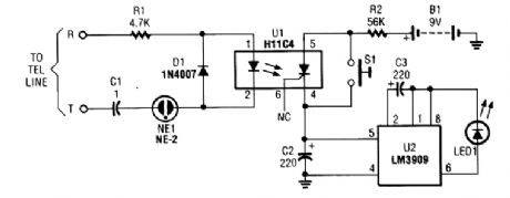
The circuit is built around a couple of low-cost ICs: an H11C4 optoisolator/coupler with an SCR output (U1) and an LM3909 LED flasher (U2). It is connected to the phone line in the same manner as any extension phone. A ring signal on the telephone activates the optoisolator/SCR, and causes U2 to flash LED1. This flash signifies that a ring signal has been received. (View)
View full Circuit Diagram | Comments | Reading(1817)
WHEATSTONE_BRIDGE
Published:2009/6/22 22:35:00 Author:May
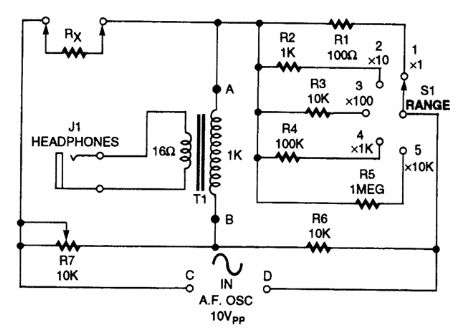

This circuit can be used to measure resistances. R7 is calibrated and fitted with an indicator dial, Lhen:
A frequency of 1 kHz for the audio oscillator is usually used. (View)
View full Circuit Diagram | Comments | Reading(1124)
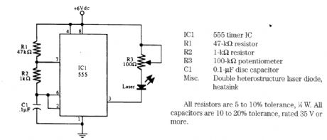
PULSED_DOUBLE_HETEROSTRUCTURE_LASER_DRIVER
Published:2009/6/22 22:34:00 Author:May
View full Circuit Diagram | Comments | Reading(847)
IC_LASER_DIODE_DRIVER
Published:2009/6/22 22:33:00 Author:May
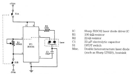
View full Circuit Diagram | Comments | Reading(1402)
MUSIC_ON_HOLD_BOX
Published:2009/6/22 22:28:00 Author:May
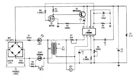
U1, an LS3404 melody chip is activated when hold S1 is pressed, which causes SCRI to con-cluct and hold the telephone line via T1, R1, and LED1. The voltage across R1 and LED1 is used to activate the melody chip. Q1 and Q2 form a restart circuit to keep the melody chip going during hold. (View)
View full Circuit Diagram | Comments | Reading(1540)
LIGHT_BEAM_RECEIVER_AND_SOUND_EFFECTS_GENERATOR_FOR_LASER_PISTOLS
Published:2009/6/22 22:27:00 Author:May
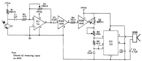
Schematic diagram for light, beam amplifier and sound-effects generator (using a 555 timer IC and speaker). The light striking Q1 generates a siren-like sound. (View)
View full Circuit Diagram | Comments | Reading(1051)
12_V_HIGH_VOLTAGE_SUPPLY_FOR_HE_NE_LASER
Published:2009/6/22 22:25:00 Author:May
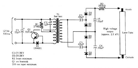
T1 is a 6-V:330-V dc/dc inverter transforlrter with a 57.4:1 turn ratio, rated at 7W.R1 270-Ω resistorR2 180-kΩ resistor, 3 to 5 W C1 22-μF electrolytic capacitorC2 1-μF electrolytic capacitorC3-C6 0.02-μF capacitor,1 kV or moreD1 1N4001 diodeD2-D5 High-voltage diode(3 kV or more)Q1 TIP 140 power transistor T1 High-voltage dc-to-dc converter transformer; see text for speciftcattons
All resistors are 5 to 10% tolerance, 1/4 W, unless otherwise indicated. All capacitors are 10 to 20% tolerance, rated 35 V or more, unless otherwise indicated. (View)
View full Circuit Diagram | Comments | Reading(2487)
EMERGENCY_TELEPHONE_DIALER
Published:2009/6/22 22:22:00 Author:May
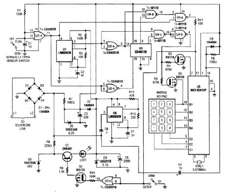
This system will alert you or anyone chosen by automatically dialing a programmed phone num-ber. This is accomplished by monitoring an open-loop or closed-loop sensor switch located in the protected area. When the sensor detects a problem (such as a break-in, fire, heating system failure, flood, etc.), Teleguard dials whatever telephone number has been programmed into its memory. When the phone is taken off the hook, Teleguard emits an unusual tone to alert the party on the re-ceiving end that something is amiss.The circuit is not hampered by busy signals when a call is placed; it automatically redials the number again and again (about once a minute) until it gets through. In addition, Teleguard can also automatically dial a number in the event of a medical emergency; for instance, where a mobility-im-paired person is unable to dial the telephone. That can be accomplished by adding a panic switch to the circuit. (View)
View full Circuit Diagram | Comments | Reading(1715)
21_GAME
Published:2009/6/22 22:21:00 Author:May
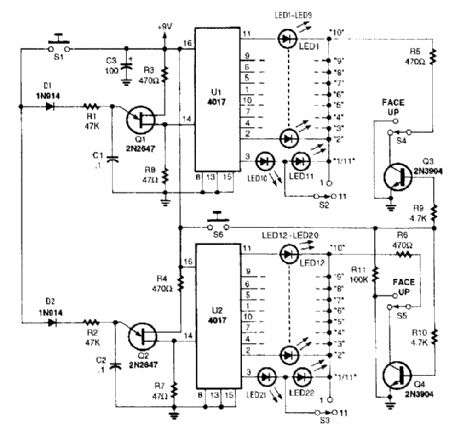


Two 2N2647 unijunction transistors serve as the Clock generators for the two 4017 ICs,A single“deal”push-button switch,S1,operates both Clock generators at the same time,Diodes D1 and D2 isolate the two Clock circuits,allowing S1 to operate both.The 4017 counter/readout circuits are identical In circuitry and operation As long as Clockpulses enter pin 14 of each 4017,the ICs count from 1 to 10 over and over until the clock pulses stopWhen S1 is released,the clock pulses stop and one LED from each IC remalns on to indicate a cardwith a number value of 1(1 or 11) to 10.The position of switches S2 and S3 determines whether the number 1 (“Ace”)output of the 4017s count as an 11 or a 1,Both S2 and S3 can be switched in either position before or after thecards are played.The cards can be played either face up OI face down,When switches S4 and S5 are in the position shown in the figure,the cards are dealt face down,Transistors Q3 and Q4 are turned off in thisposition and no current can flow through the LEDs Pressing S6 turns both transistors on,lightingthe LEDs. (View)
View full Circuit Diagram | Comments | Reading(2484)
MUSIC_ON_HOLD
Published:2009/6/22 22:14:00 Author:May
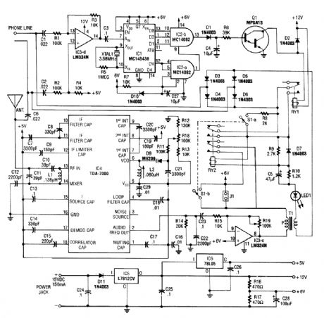
When an asterisk * is pressed on the touch-tone phone, IC1 a DTMF decoder, controls on-hold logic. Audio from the FM receiver IC4 is placed on the telephone line when a hold condition is present. RY2 is a DPDT 12-V relay. To place a caller on hold, press the asterisk button on the touch-tone phone and hang up the handset. (View)
View full Circuit Diagram | Comments | Reading(8)
TELEPHONE_RINGER
Published:2009/6/22 22:10:00 Author:May
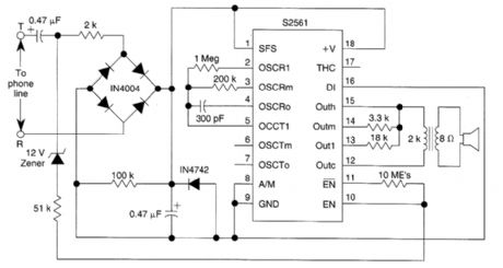
Using an AMI chip P/N S2561, this telephone ringer can be powered line. Audio output is about 50 mW when powered from a 10-V source. (View)
View full Circuit Diagram | Comments | Reading(3164)
HIGH_CURRENT_DRIVE_CIRCUIT_FOR_SINGLE_HETEROSTRUCTURE_LASER_DIODES
Published:2009/6/22 18:01:00 Author:May


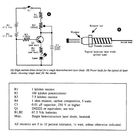
The transistor is operated in the avalanche mode. You might need to try several 2N2222 devices before finding one that oscillates. R2 is adjusted for optimum oscillation. This supply provides pulse of 10 to 20 amps at about 50 ns. (View)
View full Circuit Diagram | Comments | Reading(880)
SIMPLE_HARMONIC_DISTORTION_ANALYZER
Published:2009/6/22 17:54:00 Author:May


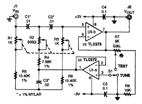
This simple circuit lets you accurately measure the total harmonic distortion(THD)using your true-RMS voltmeter.This THD circuit is somewhat different from the usual types: it can operate at the standard fre-quency of 1000 Hz, but it also is tunable from 970 Hz to 1030 Hz, and has an adjustable Q factor of 0.3 to over 50. Op-amp UI, a TLC272 CMOS unit, contains the two voltage-followers required to buffer the input to the bootstrapped twin-T notch filter. Tuning is accomplished by R1, R2, and R3, which are standard linear-taper slide pots ganged together by mounting them side-by-side and glu-ing their sliders together.The only other intportant construction hint is to use twisted pair at the cir-cuit's input and output.To calibrate the circuit, input a 1000-V RMS signal at 2000 Hz, set 51 to TEST, and adjust R7 for a reading of 0.99-V RMS on a true-RMS voltmeter at the output.To use the circuit, set 51 to TUNE, input a 1000-Hz sine-wave signal to the amplifier under test, and set the amplifier's output to the THD adapter and tune R1/R2/R3 for the lowest output signal.Then, set 51 to TEST and read the RMS voltage. To calculate the percent THD use: (View)
View full Circuit Diagram | Comments | Reading(1647)
Color TV pincushion correction circuit diagram 1
Published:2011/7/21 1:42:00 Author:Ecco | Keyword: Color TV , pincushion correction
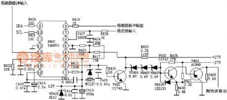
Field excitation pulses is applied directly to the pin 13 of N402 (TA8859) to trigger monostable trigger, then it generates a constant field frequency pulse-width pulse, which can control field sawtooth wave generating circuit after shaping, the N402 (15) pin is connected externally C418 capacitor with constant current charging to form a sawtooth wave current. Sawtooth amplitude and charging speed is controlled by the AGC circuit of N402, which can meet the needs of 50Hz/60Hz. Sawtooth wave produced by the field sawtooth wave circuit is made a series of linear correction by the N402, then pin (8) will output field excitation pulse.
(View)
View full Circuit Diagram | Comments | Reading(1070)
ANALOG_DE_GLITCH_CIRCUIT
Published:2009/6/19 5:13:00 Author:May
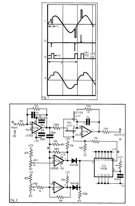


Low-frequency signals produced by transducers, measurement equipment, or data loggers often appear like the first waveform in the figure. The circuit shown operates as a tracking sample-hold, and the transients are replaced in the output by the stored value of the current signal at the instant of the transient.
The input signal is buffered and inverted by ICla, and the differentiated result shown at 2 ap-plied to the inputs of two comparators IC2-a and IC?-b. VR1 and VR2 set levels to prevent false or unnecessary operation. Either comparator output triggers the mono IC3 from positive or negative signal transients. When IC3 has not been triggered, TRI and TR2 'p' channel JFETs are on, and IClb operateb as an integrator with a high leakage, and tracks the input signal. When the mono is trig-gered as at 3, TRI and TR2 turn off and the previous signal value is held constant, as shown at 4. The resulting output waveform can then be easily filtered to remove the harmonics from the restoring step at the end of the mono period, if needed.
The criteria for successful operation are:
t2 > t1 (mono period longer than glitch)t2/T small (to optimize output waveform) Signal bandwidth Signal phase
The signal range is approximately ±5V, depending on the tfansient amplitude and polarity. The mono period shown is 100 mS, but this can be optimized in practical applications. The shorter the mono period in relation to the signal waveform, the better the quality of the result. (View)
View full Circuit Diagram | Comments | Reading(1307)
900w full-wave circuit diagram
Published:2011/7/21 3:07:00 Author:Ecco | Keyword: 900w full-wave
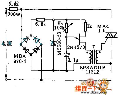
This circuitry is composed ofbidirectional triode thyristor controlled silicon delivered by unijunction transistor striking on rocks and bridge rectifier. It can provide wide range of control to resistive load by RT. The pulse transformer T makes bidirectional Hiccup controlled silicon polar and unijunction transistor steady - state current be separated.
(View)
View full Circuit Diagram | Comments | Reading(825)
VIDEO_dc_RESTORE_CIRCUIT_
Published:2009/6/19 4:58:00 Author:May
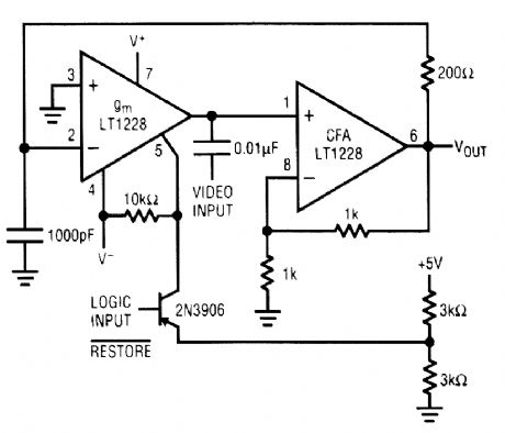
This circuit restores the black level of a monochrome composite video signal to 0 V at the beginning of every horizontal line. This circuit is also useful with CCD scanners to set the black level. (View)
View full Circuit Diagram | Comments | Reading(1349)
SIMPLE_INVERTER
Published:2009/6/19 4:52:00 Author:May
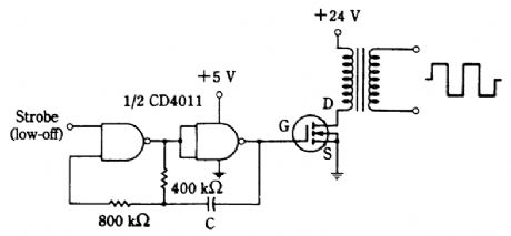
View full Circuit Diagram | Comments | Reading(852)
| Pages:347/471 At 20341342343344345346347348349350351352353354355356357358359360Under 20 |
Circuit Categories
power supply circuit
Amplifier Circuit
Basic Circuit
LED and Light Circuit
Sensor Circuit
Signal Processing
Electrical Equipment Circuit
Control Circuit
Remote Control Circuit
A/D-D/A Converter Circuit
Audio Circuit
Measuring and Test Circuit
Communication Circuit
Computer-Related Circuit
555 Circuit
Automotive Circuit
Repairing Circuit