
Basic Circuit
Index 349
FURNACE_FUEL_MISER
Published:2009/6/19 3:33:00 Author:May
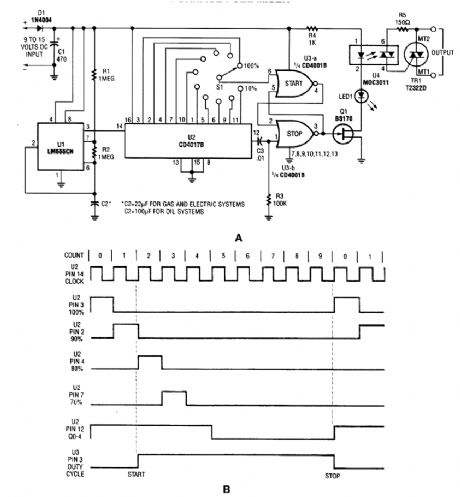
A timer (LM555CN) and decode counter is used to generate duty cycles from 10% to 100% to control the time a heating system can operate. V2 is a decode counter that can be switched from 10% to 100% duty cycle. V3A and B form a latch that drive A1, LED1, and V4. The triac TRI is used as an ac switch, in series with the thermostat that controls the heating system. (View)
View full Circuit Diagram | Comments | Reading(933)
ELECTRONIC_CRAPS_GAME
Published:2009/6/19 3:26:00 Author:May
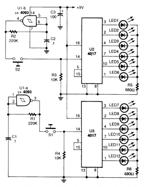
Two gates of a 4093 quad, 2-input NAND, Schrnitt-trigger CMOS IC are connected in astable-os-cillator circuits as clocks. The two 4017ICs have six LEDs connected to its first six outputs. As the clock pulses enter pin 14 of the 4017s, the ICs count from one to six over and over as long as the clock pulses are present. When S1 and/or S2 are released, one of the LEDs in each circuit will remain on, indicating a number from one to six.The circuit is set up so that you can roll the dice together by pressing S1 and S2 at the same time, or roll each die one at a time. (View)
View full Circuit Diagram | Comments | Reading(2482)
VOICE_DISGUISER
Published:2009/6/19 3:20:00 Author:May
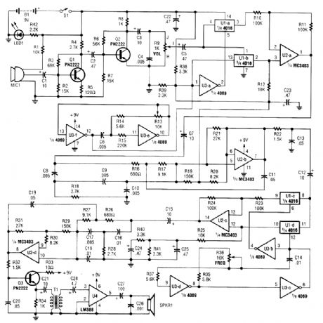
A complete schematic diagram of the voice disguiser is shown. Microphone MIC1 picks up the voice signal and feeds it to an audio amplifier, consisting of Q1 and Q2, and a few support compo-nents. The amplifier has a low-pass gain response that limits the voice frequencies to 5 kHz or lower.
The voice signal is then fed to the input of the first balanced modulator, which is comprised of U1-a, U1-b, U2-a, and U3-a. The output of the first 4-kHz oscillator, built around U3-f and U3-e, is fed to the carrier input of the first modulator. The frequency of the first oscillator is controlled by the setting of potentiometer R13. The modulator output-a double-sideband suppressed-carrier signal centered on 4 kHz-is then filtered by the first 5-kHz low-pass filter, formed by U2-b, which elimi-nates the upper-sideband signals.
At this point, the voice frequency spectrum is inverted (e.g., the frequencies that were low now become high, and vice versa), making the voice signal completely unintelligible. The output of the first low-pass filter is fed to a second modulator formed by U1-c, U1-d, and U3-b, where it is fre-quericy modulated with the output of the second carrier oscillator, comprised of U3-c and U3-d; the frequency of the second oscillator is controlled by potentiometer R36.
The output of the second modulator is filtered by the second low-pass filter, which consists of U2-d and few support components, and amplified by Q3. The voice output signal from Q3 is fed to U4 (an LM386 low-voltage, audio-power amplifier) through an impedance-matching transformer, T1.The output of U4 is then used to drive SPKR1 (an 8-Ω speaker).
In operation, if both carrier oscillators are set to the same frequency, the voice signal from the speaker will be an exact duplicate of the input signal from the microphone. However, if the frequency of the second oscillator is varied (via R36), the output voice signal also shifts in frequency. That makes the voice reproduced by the speaker sound higher- or lower-pitched than normal. (View)
View full Circuit Diagram | Comments | Reading(1441)
ACCELEROMETERG_METERCIRCUIT
Published:2009/6/19 3:09:00 Author:May
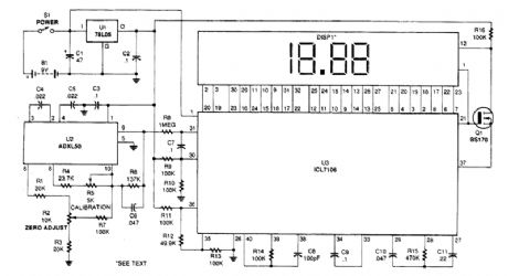
As this schematic shows,the ADXL50 accelerometer,U2,interfaces with an A/D converter,U3, to drive a 3 1/2-digit LCD module, DISPl. Because that module displays any number from -19.99 to +19.99, the circuit is designed to measure g's within that range. The heart of the circuit is U2, the ADXL50 ac-celerometer. The sensitivity of that chip is set to ±20 g's in order to accommodate the full scale capa-bility of LCD module DISP1 (19.99). Circuit gain is determined by the values of R4, R5, and R6, potentiometer R2, and R3 provides a way to manually set the zero-g voltage-output level at pin 9 of U2 to half the supply voltage-2.5V. That output voltage will vary linearly by 0.1-V/g of acceleration.In order to achieve go,od circuit performance at low g levels, the bandwidth of the amplifier is limited to about 30 Hz by C6. The digital-display section of the circuit is composed of DISP1 and U3. Included in U3 are the A/D converter, clock oscillator, storage resistors and latches, 3)6-digit seven-segment decoders, and backplane generator.The differential analog input of U3 is applied between pins 30 and 31. The positive input, pin 31, is driven by output-pin 9 of U2 through R8, a buffer resistor, and the negative input, pin 30, is biased at a fixed voltage of 2.5 V by a voltage-divider string composed of R9 and RIO.A reference voltage is required by U3. Full-scale display, 19.99, occurs when the differential, ana-log input voltage applied between pins 31 and 30 is equal to twice the reference voltage. The decimal point ofthe LCD has to be illuminated to display readings from 0.00 to 19.99. That is done by invert-ing the backplane square-wave drive signal appearing at pin 21 of U3, through MOSFET Q1, and ap-plying the 180-degree out-of-phase signal to pin 12 of DISP1. (View)
View full Circuit Diagram | Comments | Reading(4830)
Linearization circuit of thermistance
Published:2011/5/6 1:21:00 Author:May | Keyword: Linearization, thermistance
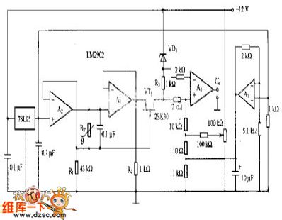
This diagram is Linearization circuit of thermistance.
In the circuit, it also is constant flow source. Its non-inverting input end is offered reference voltage by 78LO5. The output of A2 offers constant current for thermistance RT. This current is connected ground through R1. The value of constant current is determined by R1.
If RT is 5kΩ, constant current is 120μA when the voltage dropping on RT must be 0.6V. This voltage dropping adds to the source of VT1 through A3 buffer. Because the grid of VT1 is connected in one side of RT, so, grid-source voltage of VT1 is the voltage on the justified of RT. The function of R2 is flowing through idle current. The output voltage of A3 can remain unchanged when source current of VT1 changes. The justified voltage of R3 and temperature is linear relation. But R3 is in the state of floating. So, differential amplifier A4 offers this voltage. The relation between output voltage Uo and temperature changes to linear relation. (View)
View full Circuit Diagram | Comments | Reading(908)
TRIGGER_FLIP_FLOP
Published:2009/6/19 2:54:00 Author:May
Trigger flip flops are useful to divide an input frequency as each input pulse will cause the out-put of a trigger flip flop to'change state. Due to the absence of a clocking signal input, this is for an asynchronous logic application. A circuit that uses only one amplifier is shown. Steering of the dif-ferentiated positive input trigger is provided by diode CR2. For a low-output voltage state, CR2 shunts the trigger away from the (-) input and resistor R3 couples this positive input trigger to the (+) input terminal. This causes the output to switch high. The high-voltage output state now keeps CR2 off and the smaller value of (R5 + R6) compared with R3 causes a larger positive input trigger to be coupled to the (-) input, which causes the output to switch to the low-voltage state. (View)
View full Circuit Diagram | Comments | Reading(3)
With a 4 wire meet method eliminating the lead resistance effects circuit diagram
Published:2011/7/1 2:12:00 Author:Rebekka | Keyword: 4 wire meet method , lead resistance effects
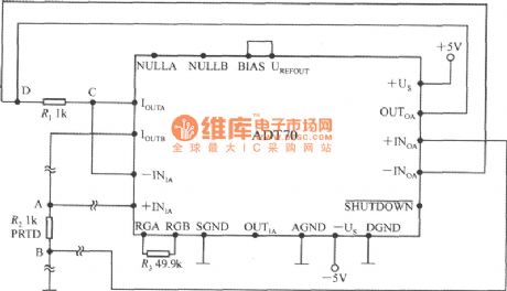
The distance measurement temperature resistance is closed to the ADT70, and its lead resistance generally can be neglected. But the leads of the platinic resistance can be up to a dozen meters and even hundreds of meters, the effects are not allow to ignore. Useing the 4 wire meet method can eliminate the influence of lead resistance. The specific circuit is shown in the figure. The characteristics of the circuit is to make the IOUTA and-INIA, IOUTB and + INIA separate from the original. It devides the line 2 into 4 connection. There are 4 nodes. Because A and C node node of the amplifier input lead has not the current, so R1, R2 lead resistance will not cause the measurement error. (View)
View full Circuit Diagram | Comments | Reading(535)
BATTERY_CHARGING_CURRENT_LIMITER
Published:2009/6/19 2:50:00 Author:May
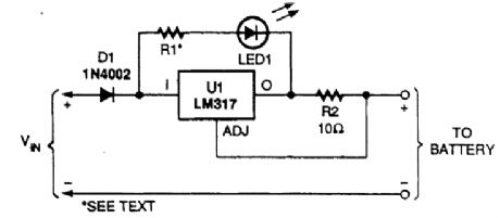
This circuit uses an LM317 as a current regulator to limit charging current to a lead-acid battery.R2 should produce a 1.2-V drop at the desired limiting value of charging current. (View)
View full Circuit Diagram | Comments | Reading(5351)
SIMPLE_LAMP_PULSER
Published:2009/6/19 2:50:00 Author:May
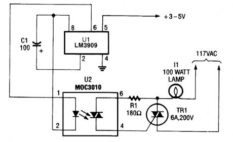
Here, the LM3090 (configured as a timing oscillator) is used to control a 117-Vac lamp through an MOC3010 optois olator/coupler. (View)
View full Circuit Diagram | Comments | Reading(2119)
SYN_COMBINER
Published:2009/6/19 2:38:00 Author:May
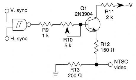
This circuit combines H and V sync signals at TTL or CMOS levels and produces an NTSC video sync output. (View)
View full Circuit Diagram | Comments | Reading(1837)
SYNC_GATINC_CIRCUIT
Published:2009/6/19 2:36:00 Author:May
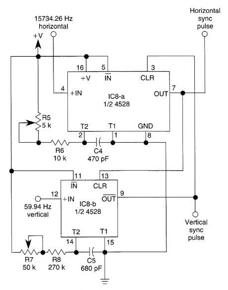
This circuit guarantees that only one type of sync pulse is generated at a time. During vertical sync periods, horizontal sync is disabled. (View)
View full Circuit Diagram | Comments | Reading(805)
SAW_FILTER_IMPEDANCE_MATCHING
Published:2009/6/19 2:34:00 Author:May
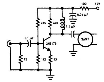
This circuit matches a saw ffiter to an IF amplifier. (View)
View full Circuit Diagram | Comments | Reading(1027)
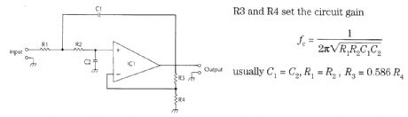
1_kHz_4TH_ORDER_BUTTERWORTH_FILTER
Published:2009/6/19 2:33:00 Author:May
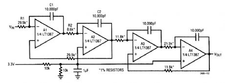


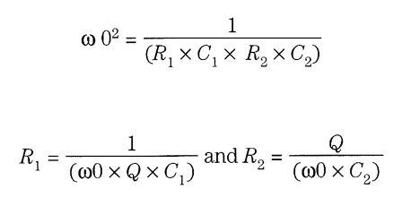
The filter is a simplified state variable architecture consisting of two cascaded 2nd-order sections. Each section uses the 360° phase shift around the two op-amp loop to create a negative sum-ming junction at Al's positive input. The circuit has low sensitivities for center frequency and Q, which are set with the following equations:where,The dc bias applied to A2 and A4, half supply, is not needed when split supplies are available.The circuit swings rail-to-rail in the passband making it an excellent anti-aliasing filter for A/Ds. The amplitude response is flat to 1 kHz then rolls off at 80 dB/decade. (View)
View full Circuit Diagram | Comments | Reading(1236)
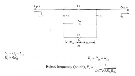
RC_NOTCH_FILTER
Published:2009/6/19 2:31:00 Author:May
View full Circuit Diagram | Comments | Reading(808)
ACTIVE_HIGH_PASS_FILTER
Published:2009/6/19 2:30:00 Author:May
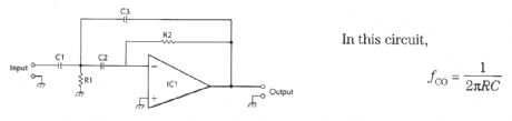
View full Circuit Diagram | Comments | Reading(0)
SALLEN_KEY_LOW_PASS_FILTER
Published:2009/6/19 2:30:00 Author:May
View full Circuit Diagram | Comments | Reading(733)
74 series digital circuit 74LS465/466 etc eight bus buffer (three state)
Published:2011/5/13 5:10:00 Author:May | Keyword: digital, eight bus buffer, three state
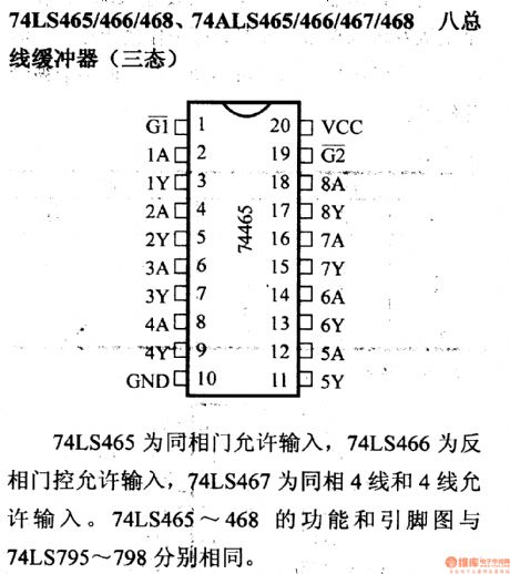
74LS465 is in-phase gatepermiting input, 74LS466 is opposite phase gate controlpermiting input,74LS467 is in-phase four lines and four linespermiting input. The function and pin diagram of 74LS465~468 is seperately same to 74LS795~798. (View)
View full Circuit Diagram | Comments | Reading(1036)
BANDPASS_FILTER
Published:2009/6/19 2:29:00 Author:May
View full Circuit Diagram | Comments | Reading(0)
20_kHz_BUTTERWORTH_ACTIVE_FILTER
Published:2009/6/19 2:29:00 Author:May

This filter will be useful for anti-aliasing or band limiting in an audio system.The op amp is a Linear Technology, LT1124,LT1355,or LT1169. (View)
View full Circuit Diagram | Comments | Reading(906)
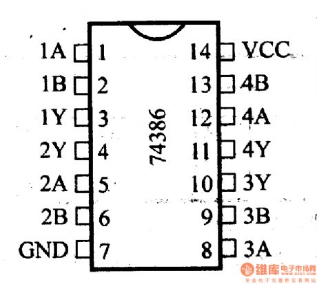
74 series digital circuit 74LS386 and other four two input XOR gate
Published:2011/5/13 5:09:00 Author:May | Keyword: digital, four two input, XOR gate

View full Circuit Diagram | Comments | Reading(1051)
| Pages:349/471 At 20341342343344345346347348349350351352353354355356357358359360Under 20 |
Circuit Categories
power supply circuit
Amplifier Circuit
Basic Circuit
LED and Light Circuit
Sensor Circuit
Signal Processing
Electrical Equipment Circuit
Control Circuit
Remote Control Circuit
A/D-D/A Converter Circuit
Audio Circuit
Measuring and Test Circuit
Communication Circuit
Computer-Related Circuit
555 Circuit
Automotive Circuit
Repairing Circuit