
Basic Circuit
Index 359
First-order active low-pass RC circuit diagram
Published:2011/7/24 22:39:00 Author:Ecco | Keyword: First-order , active low-pass RC
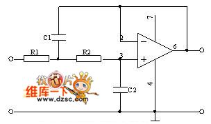
View full Circuit Diagram | Comments | Reading(607)
Second-order active low-pass RC circuit diagram
Published:2011/7/24 22:40:00 Author:Ecco | Keyword: Second-order , active low-pass RC
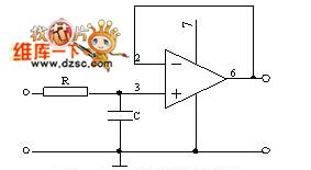
View full Circuit Diagram | Comments | Reading(533)
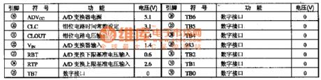
MC145162 PLL modulation integrated circuit diagram
Published:2011/7/24 21:37:00 Author:Ecco | Keyword: PLL modulation
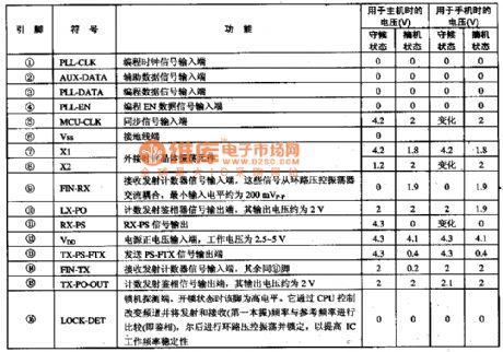
MC145162 programmable PLL frequency synthesizer modulation, demodulation IC is widely used in wireless communication receiver demodulation system. 1 Features and functionsMC145162 integrated circuit contains the transmitter and receiver signal processing circuit, clock oscillation circuit, phase-locked loop control circuit. It is mainly used to complete the wireless signal receiver, transmitter frequency controlling and locking. 2 pin functions and data MC145162 IC uses 16-pin dual in-line package, and the integrated circuit pin functions and data are listed in Table.
(View)
View full Circuit Diagram | Comments | Reading(710)
Positive converter circuit diagram composed of TDA4718
Published:2011/7/24 21:28:00 Author:Ecco | Keyword: Positive converter
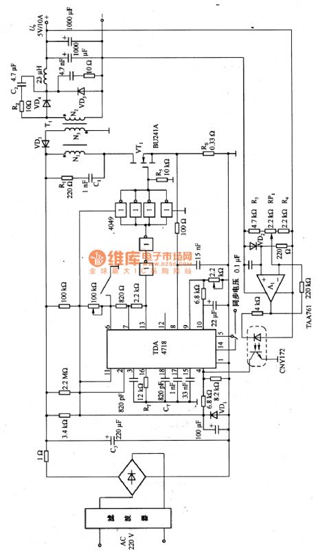
The positive converter circuit composed of TDA4718 is shown as the chart, and it can convert 220V AC voltage to 5V/10A DC output circuit. In the circuit, the tertiary winding N3, which has the same turns with the primary winding N1, can degauss the core of the transformer during VT1 deadline period, and it charges for filter capacitor C3 by the high-speed diode VD3 in order to improve the conversion efficiency. Self-resonant frequency is determined by the RT and CT. According to component parameters in the diagram, the oscillation frequency is 50kHZ.
(View)
View full Circuit Diagram | Comments | Reading(2666)
MC141628 digital comb filter integrated circuit diagram
Published:2011/7/24 21:18:00 Author:Ecco | Keyword: digital comb filter
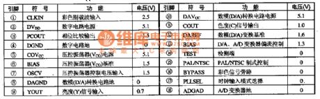
MC141628 is the digital comb filter IC produced by Motorola in America, and it is used in a wide range of domestic and imported large screen color TV, such as TCL Kleinwort series of TV and so on. MC141628 integrated circuit includes the voltage-controlled oscillator, digital-analog conversion, standard control switch, digital interface, chromaticity signal processing, clock input mode selection circuit. The lC uses 32-pin dual in-line package, and its data pin functions are listed in Table.
(View)
View full Circuit Diagram | Comments | Reading(525)
The Gate Driving Circuit Composed of TLP559
Published:2011/7/18 5:31:00 Author:nelly | Keyword: Gate Drive Circuit
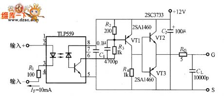
The picture is the gate driving circuit which applies the TLP559. The TLP559 output circuit is the open collector type, and VT1 does level reverse, thus the output impedance can be reduced in the complementary push-pull circuit. In order to shorten the time of open and off, the capacitor C1 which is parallel with R fastens the capacity. The value of C1 becomes large, and the admittance time becomes short, but the time of open and off becomes longer. Here,C1 selects the 4700pF. The time of open and off will be short even not connected with C1. (View)
View full Circuit Diagram | Comments | Reading(1900)
Gate Driving Half-Bridge Circuit
Published:2011/7/18 5:33:00 Author:nelly | Keyword: Gate Driving, Half-Bridge
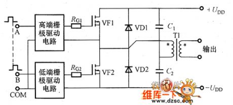
In the half-bridge circuit, the gate driving circuit can solve the below problems: the upper arm(high voltage end which is short for high end) drive need isolation; high end driving voltage always needs the voltage which is higher than power supply +UDD, namely UDD+SGS; However, it always uses the bootstrap circuit; the power MOSFET of upper and down arm can not be conducted at the same time, and the time should be predetermined. There are only two power MOSFETsin series with power supply, therefore, the diodes VD1 and VD2 are added, thus the withstand voltage of power MOSFET can close to the power supply. (View)
View full Circuit Diagram | Comments | Reading(583)
Two-way output voltage circuit diagram using MAX668
Published:2011/7/24 21:10:00 Author:Ecco | Keyword: Two-way output voltage
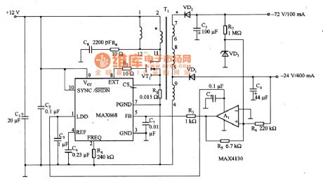
Two-way output voltage circuit using MAX668 is shown as the chart. It can convert +12 V input voltage to 72V/100mA or -24V/400mA output. The circuit is mainly composed of the MAX668 boost converter and MAX4130 op amp and transformer T1. MAX668 is the step-up controller; MAX4130 is the adder, which is used for the feedback of the two-way output voltage; the turns ratio of transformer T1 is set to 1:2:4. When the input voltage changes ± 10%, while the load changes from zero to full load, the circuit allows the two-way output voltage regulation in ± 5%.
(View)
View full Circuit Diagram | Comments | Reading(926)
μPC1406HA dual gain controller circuit diagram
Published:2011/7/24 20:49:00 Author:Ecco | Keyword: dual gain controller
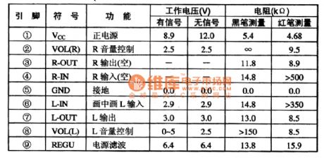
μPC1406HA dual gain controller circuit produced by Japan NEC is widely used in high-end color TV, stereo equipment. 1. Features and functions The minimum separation of μPCl406HA IC internal two attenuators is 64dB, and power supply voltage range (Vcc) is 8 to 14.4V, and supply current (Icc) is 8.5mA, and when it is Ta ≤ 75 ℃, power consumption is 35OmW. 2 pin functions and data μPC1406HA IC uses 9-pin single in-line package, and the integrated circuit pin functions and data are listed in Table 1-1.
(View)
View full Circuit Diagram | Comments | Reading(533)
DC / DC converter circuit diagram composed of NE555
Published:2011/7/24 21:57:00 Author:Ecco | Keyword: DC / DC converter
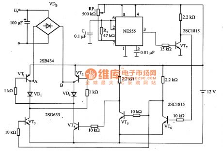
This is a converter circuit without transformer. In the circuit, power transistors VT1 ~ VT4 form the bridge circuit with alternating switch working mode, and when VT1 and VT4 are turned on, VT2 and VT3 are turned off, and it has the opposite turn in the next cycle, that is, VT2 and VT3 are turned on, and VT1 and VT4 are turned off. Bridge's A and B output AC voltage with rectangular wave, which is converted into DC voltage by the rectifier bridge VDB. NE555 is the oscillator circuit, and the oscillation frequency is decided by the R1, RP1 and C1.
(View)
View full Circuit Diagram | Comments | Reading(1447)
MC44603P switching power thick film IC diagram
Published:2011/7/24 21:51:00 Author:Ecco | Keyword: switching power , thick film IC
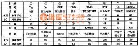
MC44603P switching power thick-film integrated circuit produced by Motorola which is widely used in Philips GFL movement (such as 28PW777A/93 TV), Philips PV4 · 0 movement (such as 25PT448A93S, 25V7, 25V8 TV), Philips MDl.OA and MDl.I movement (29PT446/93S, 29V8, etc.). 1. Features and functionsMC44603P IC contains oscillation error detection, drive, protection, synchronization control circuits. 2 pin functions and data MC44603P IC pin functions and data are listed in Table.
(View)
View full Circuit Diagram | Comments | Reading(1316)
The inverter circuit diagram composed of NE555
Published:2011/7/24 20:30:00 Author:Ecco | Keyword: inverter
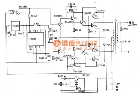
The inverter circuit diagram composed of NE555 is shown as the chart, and it can turn +12V DC battery voltage to 220V AC output voltage. In the circuit, NE555 circuit is the oscillator, the oscillation frequency is decided by the R1, RP1 and C1, and adjusting the resistance of RP1 in 50HZ, one way of the pulse signal output by NE555's pin 3 is directly added to the base of VT2, and the other way is added to the base of VT1 by passing VT11 inverter, then VT1 and VT2 get 180 ° phase difference pulse voltage.
(View)
View full Circuit Diagram | Comments | Reading(3900)
Bridging servo circuit with the TA7768F
Published:2011/7/24 20:16:00 Author:Christina | Keyword: Bridging, servo circuit
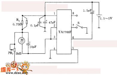
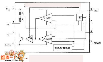
For some low voltage speed control circuits, the selection of the application-specific integrated circuit is very important, it needs to meet the requirements of the circuit such as the internal power consumption, the lowest operating voltage. The bridging servo circuit with the TA7768F is as shown in figure 1, the lowest supply voltage is 1.5V. The internal block diagram of the TA7768F is as shown in figure 2.
The adjustable resistance prt can be used in the fine tuning application of the speed. So we can use it to compensate the dispersion of the electric motor and the integrated circuit parameters.
In addition, you must notice that the small changing of the reference current is related with the dispersibility of the integrated circuit parameters. Also it is related with the variation of voltage, the load change, and the temperature change.
(View)
View full Circuit Diagram | Comments | Reading(634)
Discrete components power driver circuit diagram
Published:2011/7/24 23:33:00 Author:Ecco | Keyword: Discrete components, power driver
View full Circuit Diagram | Comments | Reading(668)
The making circuit of the small power synchronous motor governor
Published:2011/7/24 20:44:00 Author:Christina | Keyword: making circuit, small power, synchronous motor governor
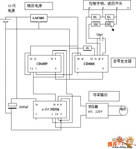
The square wave signal generator is composed of two CMOS circuits cd4060 and cd4069. The cd4060 is the oscillation and frequency division integrated circuit, the oscillation frequency is decided by the product of the capacitance (200pf) and resistance. This high frequency oscillation signal is reduced to about 50Hz through the 10 stages frequency division. The band switch of the control handle can be used to change the resistance value. In the slow stage, the two 6k resistances are connected with the rc oscillator; in the medium speed stage, one of the resistances is in the short circuit state; in the high speed stage, the two 6k resistances are in the short circuit state, the oscillation frequency is the highest.
(View)
View full Circuit Diagram | Comments | Reading(798)
Precision isolated amplifier ISO122/124 pin circuit
Published:2011/7/24 20:55:00 Author:Christina | Keyword: Precision, isolated amplifier, pin circuit
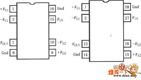
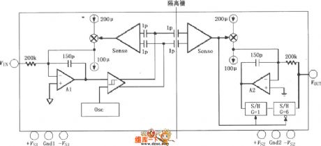
The ISO122/124 is designed as the precision isolated amplifier that has the modulation - demodulation technology of the new operating cycle. When it is sending the signal, the digital signal gets through a 2pF differential capacitance isolation fence, the isolation fence with the digital modulation characteristics will not influence the integrity of the signal, so it has great reliability and high frequency transient suppression. The two gate capacitance are embeded into the same plastic package. The ISO122/124 does not need the external components when it is operating, it has 0.02% nonlinearity, 50kHz signal bandwidth and 200μV/oC Vos drifting. The power supply range is ±4.5~±18V.
(View)
View full Circuit Diagram | Comments | Reading(1385)
12MHz broadband buffer circuit composed of the OPA606
Published:2011/7/24 21:27:00 Author:Christina | Keyword: 12MHz, broadband, buffer
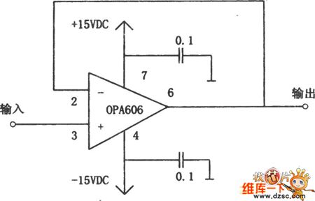
The practical broadband buffer circuit is as shown in the figure. This circuit uses the broadband integrated op-amp OPA606. The OPA606 is the MOSFET input type medium isolation operational amplifier. it has the features of wide frequency band, small bias current, low offset voltage and low distortion degree. In this figure, the input signal adds to the in-phase input port (pin-3) of the OPA606, the output port (pin-6) is connected with the inverting input port (pin-2) by the wire, the circuit forms the voltage follower, the circuit of the figure has the bandwidth of more than 12MHz, the input impedance is 1013Ω.
(View)
View full Circuit Diagram | Comments | Reading(621)
Instrument amplifier (INA101) circuit with expandable common mode range
Published:2011/7/25 1:59:00 Author:Christina | Keyword: Instrument amplifier, expandable, common mode range
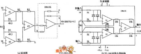
The instrument amplifier (INA101) circuit with the expandable common mode range is as shown in the figure. In this circuit, the A1, A2 and A3 are composed of the high precision instrument amplifier INA101 or INA102. In this figure, the voltage magnifications of the A1, A2 and A3 are l00 times, the post-amplifier uses the precision unit gain amplifier INA105, the connection of this amplifier is the in-phase port input and follower output model, the four resistances of the circuit are in parallel, so this INA105 amplifier can get the 2 times of voltage magnification and extremely high input impedance.
(View)
View full Circuit Diagram | Comments | Reading(1328)
HM4246 touching stepping dimmer light
Published:2011/7/20 19:04:00 Author:Lucas | Keyword: touching stepping , dimmer light
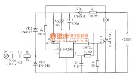
HM4246 is the touching dimmer-specific integrated circuit which is produced by Wuxi Huafang microelectronics Co., Ltd. It has 4 dimming blocks of dark, medium, light, touch to be used as zero trigger, low high-frequency harmonic radiation. It has higher touch sensitivity and stability to adapt to a longer and higher sensor board to connect the load (400pF), which is mainly used for lamps and other lighting dimming, and the circuit is shown as the chart.
(View)
View full Circuit Diagram | Comments | Reading(973)
HM9900 touching delay light circuit
Published:2011/7/20 19:03:00 Author:Lucas | Keyword: touching delay light
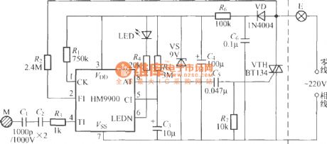
The circuit shown in the chart is the touching light delay circuit which is composed of the HM9900 specific integrated circuit, which has LED driver output usually to drive light emitting diode LED glow to look for the switch position at night.
(View)
View full Circuit Diagram | Comments | Reading(704)
| Pages:359/471 At 20341342343344345346347348349350351352353354355356357358359360Under 20 |
Circuit Categories
power supply circuit
Amplifier Circuit
Basic Circuit
LED and Light Circuit
Sensor Circuit
Signal Processing
Electrical Equipment Circuit
Control Circuit
Remote Control Circuit
A/D-D/A Converter Circuit
Audio Circuit
Measuring and Test Circuit
Communication Circuit
Computer-Related Circuit
555 Circuit
Automotive Circuit
Repairing Circuit