
Basic Circuit
Index 345
DDS_DIGITAL_VFO
Published:2009/6/23 1:58:00 Author:May
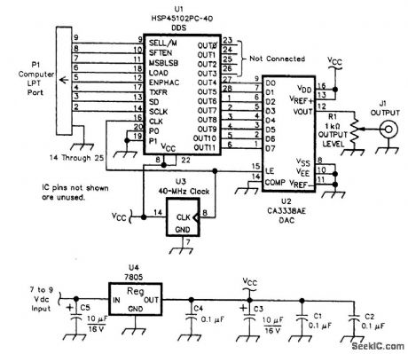
The DDS chip (U1) generates a data stream that is converted by D/A converter U2 into a sine wave. U1 is programmed via the input from P1, from the LPT port of an IBM PC. The system uses a 40-MHz TTL output clock module. (View)
View full Circuit Diagram | Comments | Reading(1150)
POWER_BOOSTER
Published:2009/6/23 1:57:00 Author:May
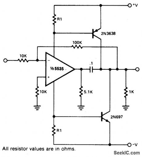
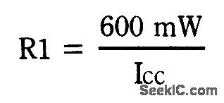
Power booster is capable of driving mod-erate loads. The circuit as shown uses a NE5535 device. Other amplifiers may be sub-stituted only if R1 values are changed because of the ICC current required by the amplifier. R1 should be calculated from the following ex-pression: (View)
View full Circuit Diagram | Comments | Reading(0)
ac_LINE_VOLTAGE_BOOSTER
Published:2009/6/23 1:54:00 Author:May
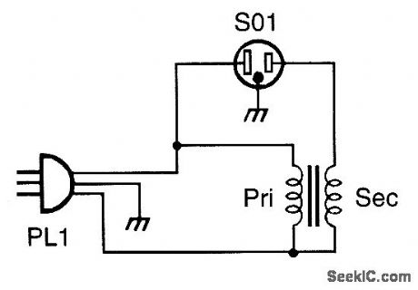
When incoming ac power drops, you can bring the voltage back up with this booster circuit. It adds the transformer's secondary voltage to the ac line voltage. (View)
View full Circuit Diagram | Comments | Reading(1402)
FET_VXO_CIRCUIT
Published:2009/6/23 1:49:00 Author:May
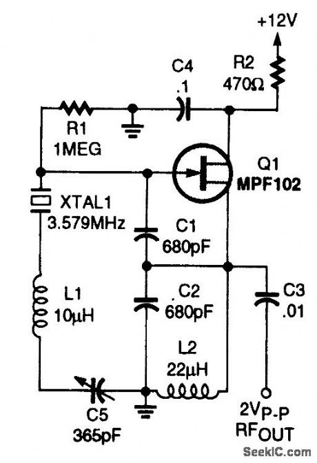
An MPF 102 is used in a Colpitts-type oscilla-tor in order to pull the crystal frequency slightly. (View)
View full Circuit Diagram | Comments | Reading(0)
dc_OUTPUT_CHOPPER
Published:2009/6/23 1:49:00 Author:May
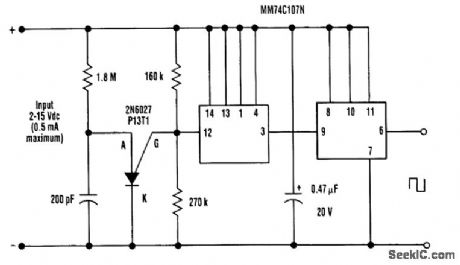
Any dc voltage source in the 2- to 15-V range can be chopped into a unipolar square wave that has a peak amplitude nearly equal to the dc source voltage with circuit (lightly loaded CMOS will swing within a few millivolts of each rail at low frequencies). Depending on the actual voltage of the supply, the programmable-unij unction-transist or (PUT) relaxation oscillator produces 2000-Hz trigger pulses. These pulses operate the cascaded 74C107 flip-flop, producing a square wave. (View)
View full Circuit Diagram | Comments | Reading(0)
SUBAUDIBLE_TONE_ENCODER
Published:2009/6/23 1:48:00 Author:May
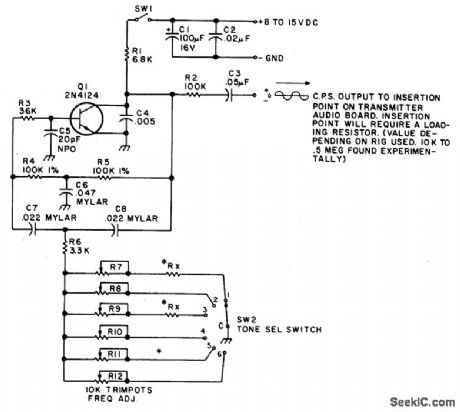
This twin-T oscillator produces six preset subaudible tones from 93 to 170 Hz in three ranges. (View)
View full Circuit Diagram | Comments | Reading(0)
VARIABLE_FREQUENCY_ASTABLE_II
Published:2009/6/23 1:43:00 Author:May
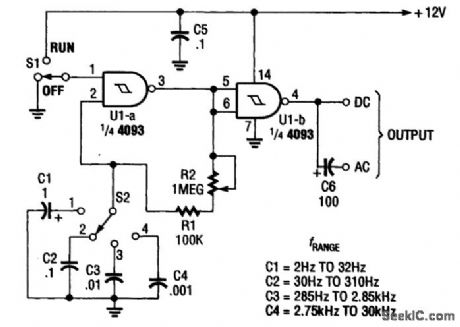
This circuit uses a single potentiometer and switched capacitors to cover 2 Hz to 30 kHz。 (View)
View full Circuit Diagram | Comments | Reading(0)
TEA2260 thick film switching power IC diagram
Published:2011/7/27 21:19:00 Author:Ecco | Keyword: thick film , switching power IC
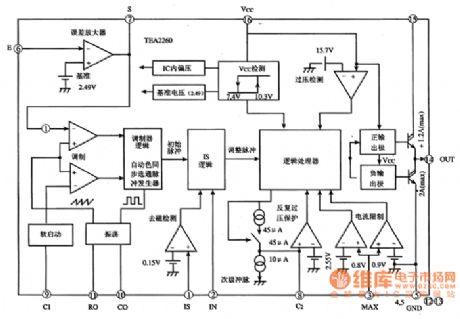
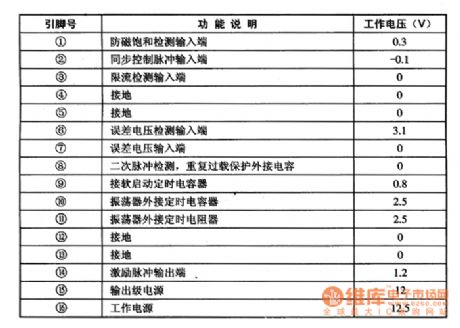
TEA2260 thick film switching power integrated circuit produced by French Thomson company is widely used in large-screen color television sets and computer monitors, switching power supply circuits. 1.The internal block diagram The internal block diagram of TEA2260 integrated circuit is shown in Figure 1. 2. pin functions and data TEA2260 IC uses 16-pin double row package, and the pin functions and data are listed in Table 1.
(View)
View full Circuit Diagram | Comments | Reading(1172)
VARIABLE_FREQUENCY_ASTABLE_I
Published:2009/6/23 1:37:00 Author:May
This Circuit is a variable frequency oscillator usming a trimmer capacitor or a three-gauge AM broadcast capacitor salvaged from an old AM radio. The there sections must be paralleled. (View)
View full Circuit Diagram | Comments | Reading(978)
Three-band graphic equalizer
Published:2011/7/28 20:34:00 Author:Ecco | Keyword: Three-band graphic equalizer
Using a single op-amp this easy to make equalizer offers three ranges, low frequency,mid frequency,and high. With component values shown there is approximately +/-20dB of boost or cut at frequencies of 50Hz, 1kHz and 10kHz. Supply voltage may be anything from 6 to 30 Volts. Maximum boost 20dB is only realized with maximum supply voltage. (View)
View full Circuit Diagram | Comments | Reading(1104)
CW_SIGNAL_PROCESSOR
Published:2009/6/23 1:36:00 Author:May
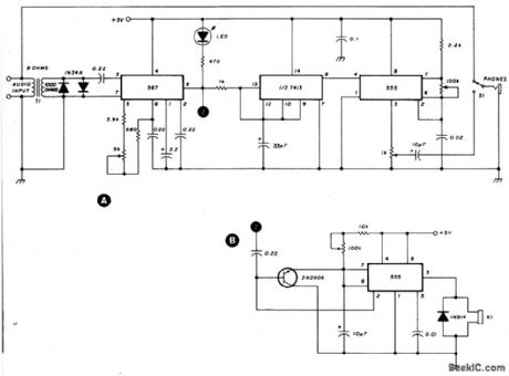
This circuit provides interferenced rejection for the CW operator. The 567 phase-locked loop is configured to respond to tones from 500 to 1100 Hz. The Schmitt trigger reduces the weighting effect caused by the output of the PLL remaining low after removal o f the audio signal. Ten to 15 millivolts of audio activate the circuit. For periods of loss of signal, circuit B will automatically switch back to live receiver audio after a suitable delay. (If a relay with a 5-volt coil is not available, the circuit can also be powered from +12 volts.) When circuit B is used, the contacts on relay K1 replace S1. (View)
View full Circuit Diagram | Comments | Reading(1158)
GATED_2_kHz_BUZZER
Published:2009/6/22 23:56:00 Author:May
View full Circuit Diagram | Comments | Reading(683)
A SCR exchanging switch circuit diagram
Published:2011/7/28 2:53:00 Author:Ecco | Keyword: SCR , exchanging switch
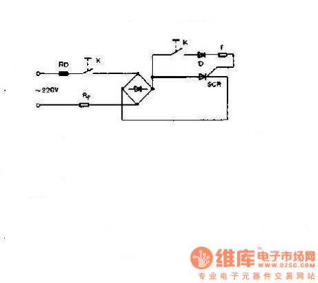
The SCR is the switch of electrical equipment,which is used to conduct and cut off the electric, andit has the advantages of no contact beating and arc, small mechanical noise and radio frequency interference, high switching speed and small size. It's suitable for dangerous places with flammable gas which could cause explosion easily. The circuit is shown as the chart: It is a simple SCR exchanging switch circuit. When switch K closes, SCR turns on, the value of R generally selects thousands of Ω.
(View)
View full Circuit Diagram | Comments | Reading(548)
DITHERIZER
Published:2009/6/22 23:54:00 Author:May
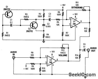
In digital audio, a noise signal of amplitude less than one significant bit is often added to the au-dio to reduce the quantizing effect and improve the audio quality by trading digital noise for ana-log noise, which does not have the harsh sound. This circuit consists of a noise generator to add a low level of noise to an analog signal to be digitized, or an analog signal from a digital source. (View)
View full Circuit Diagram | Comments | Reading(0)
SIMPLE_INTERCOM_FOR_NOISY_ENVIRONMENTS
Published:2009/6/22 23:51:00 Author:May
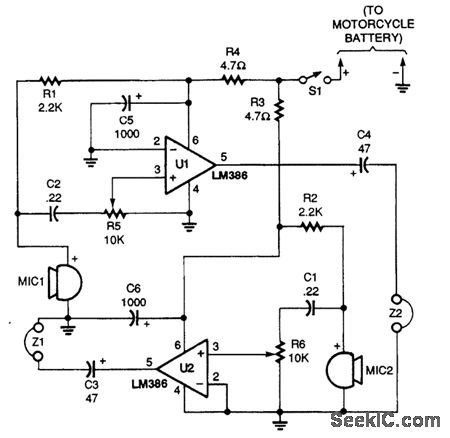
This intercom was originally designed for motorcycle to passenger communications A simple"passenger-to-pilot”ttercom circuit is shown. Two LM386 ICs are connected in a low-gam amplifiercircuit with the headphone output of one paired to the microphone input of the other The microphones are electret elements and the earphones can be of the in-ear type or of the small stereo/monotype that with fit inside a helmet Both amplifiers in the circuit operate at a minimum gain of 20 dB. (View)
View full Circuit Diagram | Comments | Reading(0)
225_W_15_V_OUTPUT_CONVERTER_20_kHz_inverter
Published:2009/6/22 23:47:00 Author:May
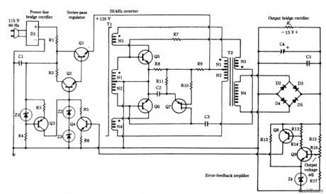
A converter designed to supply t15 Vdc is shown. This converter is several times lighter in weight than an equivalent.
C1 -2500 μF,350 V Electrolyic Q1,Q5,Q6,-2N6307C2—0.1μF Disc Ceramic Q2,Q4 - 2N5052C3—0.1μF Paper Q3—2N5345C4—10 μF Electrolylc Q7-2N4870C5—0.25μF Paper Q8 -2N3905D1—MDA-980-4 Bridge Rectifier Assembly Q9—2N3903 D2,D3,D4,D5-1N5826,20V 15A
All Resistors in Ohms and 1/2 W Unless Otherwise Noted
R1—1,10 W R10-1KR2-100 R11-10KR3-82R12-270R4- 22K R13-1KR5-1.5K,15W R14-7.5KR6-200 R15-2.5KR7-15 R16-5KR8—4.7K 17-3.5KP9-51
T1 - Core -Magnetics Inc 80623-1/2 D-080N1,N2-20 Turns Each,No 30 AWG(Bifilar)N3,N4- 3 Turns Each,No 20 AWG
T2—Core—Arnold 6T 5800 D1N1,N2-100 Turns Each,No. 20 AWG(Bifilar)N3-7 Turns No. 20 AWGN4-12 Turns Each No 12 AWG(No 16 AWG,3 In Parallel)
Z1 —1N4733,5.1 VZ2,Z3 -1N4760,68VZ4- 1N4736 (View)
View full Circuit Diagram | Comments | Reading(982)
Active / Passive Phono Preamplifier Circuit
Published:2011/7/18 6:00:00 Author:Felicity | Keyword: Active / Passive Phono, Preamplifier Circuit
View full Circuit Diagram | Comments | Reading(1343)
PSEUDOGROUND
Published:2009/6/22 23:37:00 Author:May
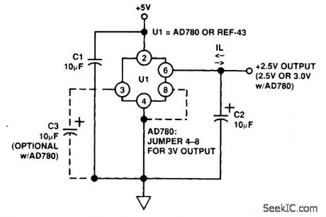
For op-amp circuits, a pseudo ground is often needed; a voltage reference IC can be used. The Analog Devices AD780 is used here for this application. This can sink or source current. (View)
View full Circuit Diagram | Comments | Reading(0)
SINGLE_CHIP_MESSAGE_SYSTEM
Published:2009/6/22 23:35:00 Author:May
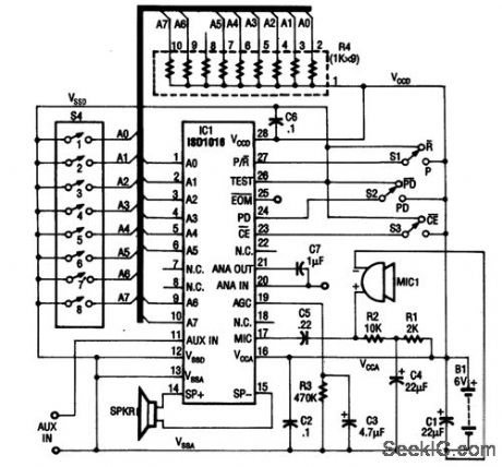
The ISD1016 is a complete analog audio record/playback system on a chip. The analog signal is sampled and the samples stored in an EEPROM as analog levels. Upon playback, the analog data is read out and amplified. Up to 16 seconds of data(audio)can be stored. (View)
View full Circuit Diagram | Comments | Reading(0)
SHORT_CIRCUIT_BEEPER
Published:2009/6/22 23:33:00 Author:May
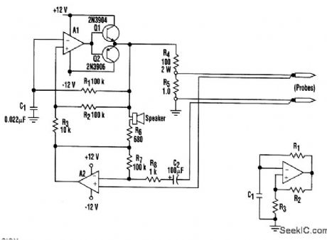
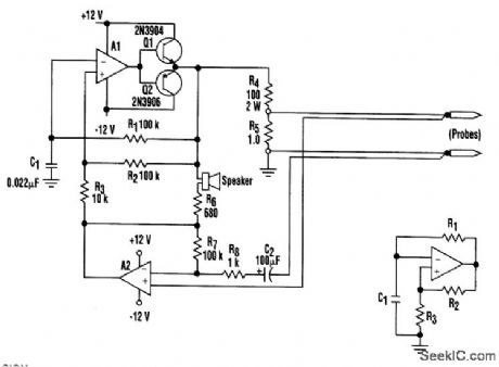
This design offers a way to trace resistance in the milliohm range, right to a short between bridged traces beneath a solder mask. It simply translates resistance into an audible tone, which in-creases in pitch as the measured value approaches zero.In the classic op-amp multivibrator (shown in the inset), oscillation frequency is determined not only by the R1/C1 time constant, but also by the hysteresis set by the R2/R3 resistance ratio. Al in the main figure, with current boosters Q1 and Q2, is this same configuration.Assuming a virtual ground at the output of A2, free-run frequency is about 1 kHz-quite audible through a tiny 8-Ω speaker. Q1 and Q2 deliver a ±10-V squarewave to R4, dumping a ±100 mA through a short circuit placed across the probe tips. R5 ensures that open circuit voltage never ex-ceeds ±0.1 V.AZ monitors the voltage between the probes. The differential input must have its own separate path to the probe tips to eliminate test lead resistance from the measurement. Miniature zip-cord sold as loudspeaker wire makes a tidy two-conductor test lead.When the probes are open, A2's gain equals the R4/R5 divider loss, and the output of both am-plifiers is identical. This has two effects: first, hysteresis is greatly increased and the frequency falls to a low growl; second, the loudspeaker that bridges the two in-phase outputs is effectively silenced.The dead short across the probe tips will return nothing to AZ and the circuit will squeal at its nominal 1-kHz rate. Anything less than a perfect short produces some output from A2, increasing multivibrator hysteresis and lowering the pitch. The circuit has so much 'leverage, and the ear is so sensitive to pitch changes in this range, that it's easy to resolve minute resistance differences.Any general-purpose op amp will suffice in this circuit-a couple of 741s or an equivalent dual. (View)
View full Circuit Diagram | Comments | Reading(957)
| Pages:345/471 At 20341342343344345346347348349350351352353354355356357358359360Under 20 |
Circuit Categories
power supply circuit
Amplifier Circuit
Basic Circuit
LED and Light Circuit
Sensor Circuit
Signal Processing
Electrical Equipment Circuit
Control Circuit
Remote Control Circuit
A/D-D/A Converter Circuit
Audio Circuit
Measuring and Test Circuit
Communication Circuit
Computer-Related Circuit
555 Circuit
Automotive Circuit
Repairing Circuit