
Basic Circuit
Index 343
FAST_33_V_REGULATOR
Published:2009/6/23 3:45:00 Author:May
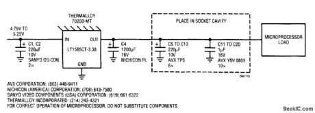


New high-performance microprocessors require a fresh look at power-supply transient response.The LT1585 linear regulator features 1% initial accuracy, excellent temperature drift and load regulation, and virtually perfect line regulation. Complementing superb dc characteristics, the LT1585 exhibits extremely fast response to transients. Transient response is affected by more than the regulator itself. Stray inductances in the layout and bypass capacitors, as well as capacitor ESR dominate the response during the first 400 ns of transient.The ftgure shows a bypassing scheme developed to meet all the requirements for the Intel P44C-VR microprocessor. Input capacitors C1 and C2 function primarily to decouple load transients from the 5-V logic suppJy. The values used here are optimized for a typical 5-V desktop computer silver box powersupply input. C5 to C10 provide bulk capacitance at low ESR and ESL, and C11 to C20 keep the capacitance at low ESR and ESL low at high (>100 kHz) frequencies. C4 is a damper and it minimizes ringing during setting. Trace C is the load current step, which is essentially flat at 4 A with a 20-ns rise time.Trace A is the output settling response at 20 mV per division. Cursor trace B marks -46 mV relative to the initial output voltage. At the onset of load current, the microprocessor socket voltage dips to -38 ntV as a result of inductive effects in the board and capacitors, and the ESR of the capacitors. The inductive effects persist for approximately 400 ns. For the next 3 μs, the output droops as the load current drains the bypass capacitors. The trend then reverses as the LT1585 catches up with the load demand, and the output settles after approximately 50 μs. Running 4 A with a 1.7-V drop, the regulator dissipates 6.8 W. (View)
View full Circuit Diagram | Comments | Reading(0)
GROUND_LOOP_PREVENTER
Published:2009/6/23 3:32:00 Author:May
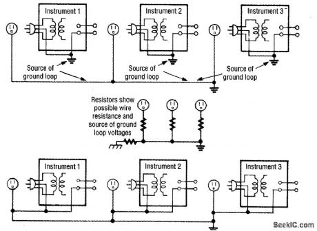
Ground loops are caused by improper grounding. Ground-loop voltages can interfere with test rrteasurements because the voltages in a ground loop can be larger than the signals you're trying to measure. To prevent ground loops, use two wire plugs to provide the line power to the test instru-ments and a separate wire to bring the input grounds of the instruments to a common ground. (View)
View full Circuit Diagram | Comments | Reading(0)
JACOB’s_LADDER
Published:2009/6/23 3:28:00 Author:May
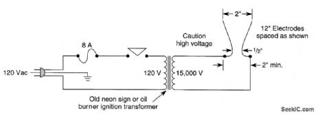
A“Iacobs Ladder”can be made from an old neon sign or oil burner ignition transformer. A rating of 12 to 15 kV at 20 to 30 mA will be adequate. Make sure to mount the electrodes to a pair of in-sulators, at least 2 apart, and bent and spaced, as shown. The ladder should be enclosed in a clear plastic housing to prevent accidental contact with the high voltage and to ensure a stable arc. Vent holes should be placed top and bottom to allow gases to escape. (View)
View full Circuit Diagram | Comments | Reading(2774)
CURRENT_LIMITING_REGULATOR_CIRCUIT
Published:2009/6/23 3:25:00 Author:May
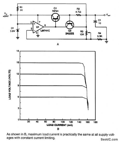

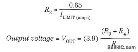
This regulator uses the drop across R2 to turn on Q2, removing base drive from Q1 and reducing the current through R1. About 0.65 V must be dropped across R2 before limiting occurs. To set limit current, (View)
View full Circuit Diagram | Comments | Reading(1258)
About TLC5941 Dynamic Scanning Drive Circuit
Published:2011/7/23 8:12:00 Author:Michel | Keyword: Dynamic Scanning, Drive Circuit
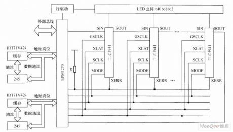
Here we introduce 640 x 480 full-color display system driving part design.The whole screen is composed of 4 subscreens and every subscreen manages 640 x 120 pixel range and they have single driving circuit.Because it is inner screen ,the driving design adopts dynamic scanning driving way.Drive circuit control is realized by programmable logic devices EPM1270 (Altera).
In order to improve the frame frequency, serial data uses 15 groups parallel output and every group refreshes 640 x 120 pixel range.The figure 1 shows the subscreen's single circuit.
(View)
View full Circuit Diagram | Comments | Reading(567)
×10_FREQUENCY_MULTIPLIER
Published:2009/6/23 3:23:00 Author:May
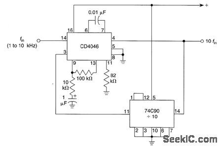
In this circuit, the CD4046 is set up so that the VCO operates at 10 to 100 kHz. The output pin(4) is fed back to a ÷10 counter. When the input frequency is 1/10 the output, lockup will occur. (View)
View full Circuit Diagram | Comments | Reading(3167)
POSITIVE_FEEDBACK_CABLE_TERMINATOR
Published:2009/6/23 3:18:00 Author:May
Positive feedback along with a series output resistor can provide a controlled output impedance from an op-amp circuit. The circuit is useful when driving coaxial cables that must be terminated at each end in their characteristic impedance, which is often 50Q. Adding a 50-Q series resistor on the op amp's output obviously reduces the available signal swing. (View)
View full Circuit Diagram | Comments | Reading(0)
Level 4 Telecom Filter Circuit of uA741 Op-amp
Published:2011/7/22 21:56:00 Author:Michel | Keyword: Op-amp, Level 4, Telecom, Filter Circuit
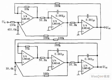
The above circuit can use common calculation formula and then the total requirements are divided into several sections:Q1=0.541,Q2=1.306.This circuit adopts LM148 or 741 four operational amplifier. (View)
View full Circuit Diagram | Comments | Reading(929)
455_kHz_MODULATOR
Published:2009/6/23 3:10:00 Author:May
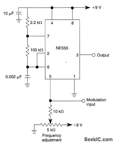
This circuit shows how to frequency-modutate the oscillator using a 555. Oscillator frequency is set with the 5-kΩ potentiometer and the modulation signal is dc-coupled. (View)
View full Circuit Diagram | Comments | Reading(0)
FM_MODULATOR
Published:2009/6/23 3:08:00 Author:May
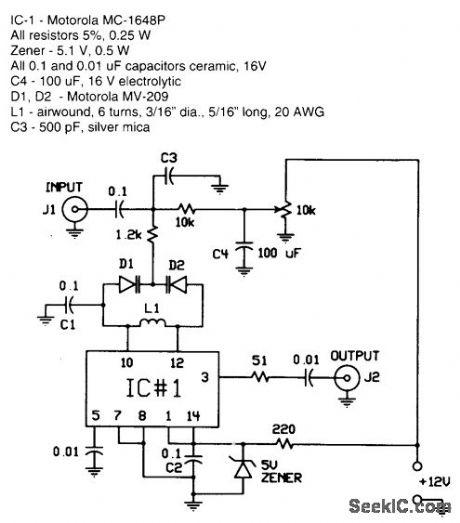
The FM modulator is built with a Motorola MC1648P oscillator. Two varactors, Motorola MV209, are used to frequency modulate the oscillator. The 5000-Ω potentiometer is used to bias the varactors for best linearity. The output fre-quency of approximately 100 MHz can be ad-justed by changing the value of the inductor. The output frequency can vary as much as 10 MHz on each side. The output level of the modulator is -5 dBm. In this prototype, the varactor bias was 7.5 V for best linearity; but this could be different with other varactors. (View)
View full Circuit Diagram | Comments | Reading(0)
Capacitor circuit diagram in capacitor dropping vlotage source
Published:2011/7/20 20:18:00 Author:Ecco | Keyword: Capacitor , capacitor, dropping vlotage, source
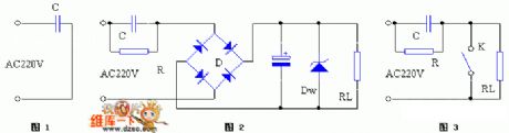
In the commonly low-voltage power supply, comparing with the transformer, the capacitor dropping vlotage source has the advantages of small size, economical, reliable, high efficiency, the disadvantage is that the safety is not as good as the power transformer. The AC is leaded to the load by the capacitor, then it has 220V voltage on the ground, which will cause electric shock easily, but if the circuit is used in the internal circuit power supply which has no human contact, this weakness can be overcome. For example, the refrigerator thermostat or remote control of electronic power supply, etc. are all open ╱ off by the capacitor dropping vlotage source.
(View)
View full Circuit Diagram | Comments | Reading(497)
UNITY_GAIN_FOUR_INPUT_AUDIO_MIXER
Published:2009/6/23 3:02:00 Author:May
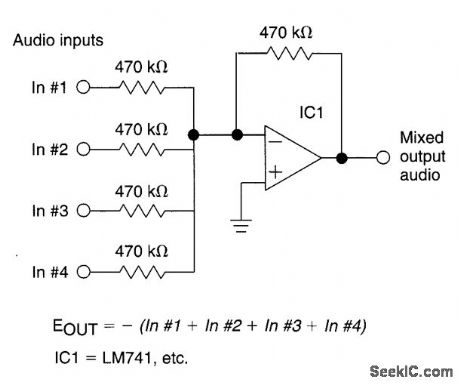
The circuit has four inputs. The voltage gain between each input and the output is held at unity by the relative values of the 470kΩ input resistor and the 470kΩ feedback resistor. (View)
View full Circuit Diagram | Comments | Reading(1105)
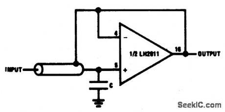
PRECISION_AVSOLUTE_VALUR_CIRCUIT
Published:2009/6/23 3:02:00 Author:May
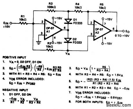
View full Circuit Diagram | Comments | Reading(629)
Switching elements on-off speed controller circuit diagram
Published:2011/7/20 20:19:00 Author:Ecco | Keyword: Switching elements , on-off , speed , controller
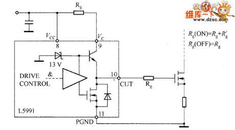
Pin 9 (VC) is used for the promotion of external switching devices. In order to avoid the effect on the pin from the pulse current effect, it should be connected a buffer capacitor between the pin and the ground (pin 11) to suppress interference caused by the current pulse. In addition, in order to adjust the external switching components on-off speed, it could be added a resistor between the buffer capacitor and pin, and the circuit is shown in Figure 9-36. From the figure, we can see, when power MOSFET gate is turned on, the resistance is Rg + R'g, and when it is turn-off, the gate resistance is only Rg.
(View)
View full Circuit Diagram | Comments | Reading(638)
CONTACT_DEBOUNCER
Published:2009/6/23 3:00:00 Author:May
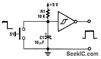
A contact debouncer using a Schmitt trigger, such as a TTL7414, provides a clean pulse from a switch contact closing. (View)
View full Circuit Diagram | Comments | Reading(776)
PIEZOELECTRIC_DRIVER_CIRCUIT
Published:2009/6/23 2:59:00 Author:May
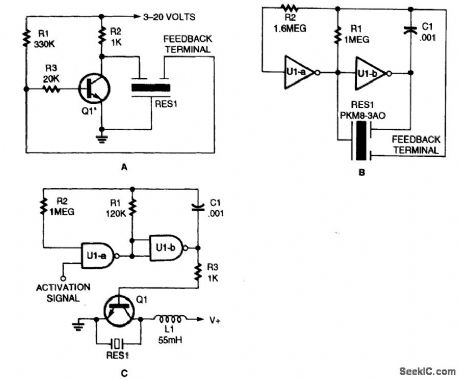
Three-terminal piezoelectric elements are typically driven by transistor circuits (A), or logic gates (B). Two-terminal devices can be driven by two NAND gates. A booster coil is used to compensate for the sound-pressure attenuation caused by the case. (View)
View full Circuit Diagram | Comments | Reading(1)
FET_MICROPHONE_MIXER
Published:2009/6/23 2:59:00 Author:May
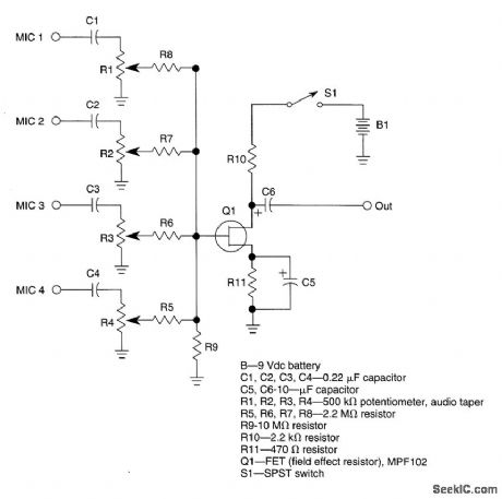
A JFET transistor is used as a high-to-low impedance converter and signal mixen Input impedance is approximately 500 kΩ but it can be increased by increasing R5 to R8 as high as 10 MΩ. Output Z is about 2 kΩ, but it can be increased or decreased by changing the value of R10 Use 560 or 680 Ω to feed a 600-Ω input; use 100 kΩ to 1 MΩ for high irnpedance. (View)
View full Circuit Diagram | Comments | Reading(1049)
74 series digital circuit of 7450, 74H50 dual 2 input and-nor gate
Published:2011/7/21 3:08:00 Author:Ecco | Keyword: digital circuit , 2 input , negater
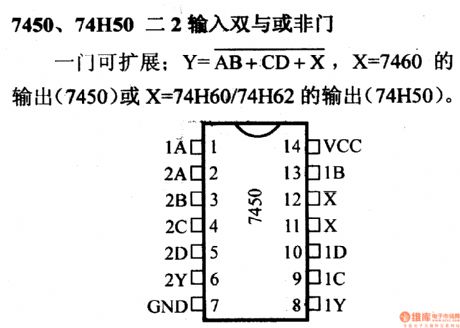
7450, 74H50 dual 2 input and-nor gate
(View)
View full Circuit Diagram | Comments | Reading(689)
CURRENT_BOOSTER
Published:2009/6/23 2:48:00 Author:May
View full Circuit Diagram | Comments | Reading(638)
CABLE_BOOTSTRAPPING
Published:2009/6/23 2:47:00 Author:May
Bootstrapping input shield for a follower reduces cable capacitance, leakage, and spurious voltages from cable flexing. Instability can be avoided with small capacitor on input. (View)
View full Circuit Diagram | Comments | Reading(818)
| Pages:343/471 At 20341342343344345346347348349350351352353354355356357358359360Under 20 |
Circuit Categories
power supply circuit
Amplifier Circuit
Basic Circuit
LED and Light Circuit
Sensor Circuit
Signal Processing
Electrical Equipment Circuit
Control Circuit
Remote Control Circuit
A/D-D/A Converter Circuit
Audio Circuit
Measuring and Test Circuit
Communication Circuit
Computer-Related Circuit
555 Circuit
Automotive Circuit
Repairing Circuit