
Basic Circuit
Index 404
Static electricity eliminator circuit diagram 2
Published:2011/6/9 4:08:00 Author:Lucas | Keyword: Static electricity eliminator
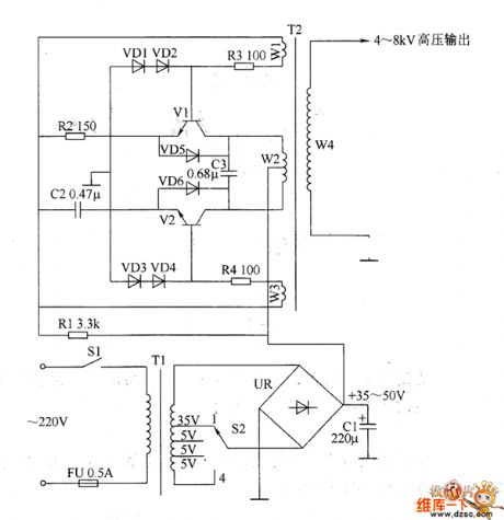
The static electricity eliminator circuit is composed of the power circuit and oscillation step-up circuit, and the circuit is shown as the chart. Power circuit consists of the power switch S1, fuse FU, power transformer T1, bridge rectifier UR, filter capacitor C1 and voltage selecting switch S2. Oscillation step-up circuit consists of the resistors R1 ~ R4, capacitors C2 and C3, diodes VD1 ~ VD6, step-up transformer T2 and transistors VI, V2. R1 selects lW metal film resistor; R2 ~ R4 select 1/4W metal film resistors. C1 uses aluminium electrolytic capacitor with the voltage in 63V: C2 and C3 select the CBB capacitors with the voltage in 250V. VD1 ~ VD4 use 1N4007 silicon rectifier diodes; VD5 and VD6 use 1N5406 silicon rectifier diodes.
(View)
View full Circuit Diagram | Comments | Reading(2558)
Welder no-load power saver circuit diagarm 8
Published:2011/6/10 5:41:00 Author:Lucas | Keyword: Welder, no-load , power saver
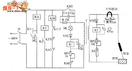
The welder no-load power saver circuit is composed of the knife switch Q, relays K1 and K2, relay KA, AC contactor KM, time relay KT, reed SA, diodes VD1 and VD2, LED HL, resistor R, capacitors C1 ~ C3, potentiometers RP1 and RP2 and the welding transformer T, and the circuit is shown as the chart. R uses 1/4W metal film resistor. RP1 and RP2 use 2W wire-wound resistors. C1 uses the CBB capacitor with the voltage being 630V; C2 uses the aluminium electrolytic capacitor with the voltage being 50V; C3 uses the aluminium electrolytic capacitor with the voltage being 16V. VD1 and VD2 use 1N4007 silicon rectifier diodes. KA uses the intermediate relay with the coil voltage selection 380V (or 220V) AC.
(View)
View full Circuit Diagram | Comments | Reading(1390)
Welder no-load power saver circuit diagarm 7
Published:2011/6/10 5:35:00 Author:Lucas | Keyword: Welder , no-load , power saver
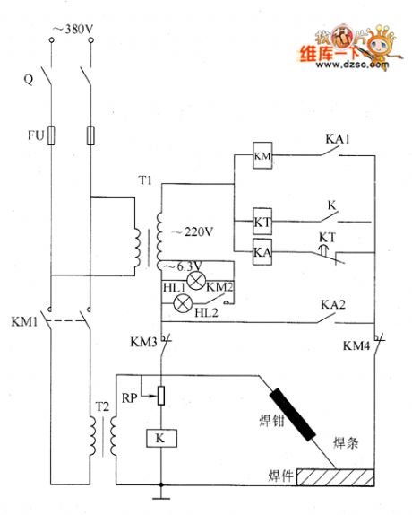
The welder no-load power saver circuit is composed of the power transformer T1, intermediate relay KA, relay K, time relay KT, AC contactor KM, potentiometer RP and indicator lights H12, HL1, and the circuit is shown as the chart. Knife switch Q, fuse FU, welder transformer T2 form the main circuit of original welder. RP uses 2W wire-wound resistor. HL1 and HL2 select 1W, 6.3V lights. KA chooses the intermediate relay with the contact current capacity being greater than 5A, coil voltage being 220V AC. KT selects the time relay with the coil voltage being 220V AC, such as the JS11 series. KM uses 220V AC coil voltage contactor. Q, FU, and KM's contact current capacity should be based on reasonable selection of real power.
(View)
View full Circuit Diagram | Comments | Reading(986)
Welder no-load power saver circuit diagarm 6
Published:2011/6/10 5:07:00 Author:Lucas | Keyword: Welder , no-load , power saver
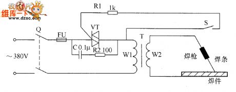
The welder no-load power saver circuit is composed of the knife switch Q, fuse FU, capacitor C, resistors R1 and R2, thyristor VT, welding transformer T and the trigger switch S, and the circuit is shown as the chart. Q, FU, VT, and T form the main circuit of the welder, and S, R1, and VT form the power saving switching circuit; C and R2 form the current limiting circuit. Before the the trigger switch S being connected, VT is in the off state. R1 selects 1/2W metal film resistor; R2 uses 1OW cement resistor. C selects the CBB capacitor with the voltage being 400V. VT uses 30 ~ 50A, 600V directional triode thyristor. S uses the micro switch or small normally open button. The choices of FU and Q should be based on the actual power of T.
(View)
View full Circuit Diagram | Comments | Reading(1640)
Welder no-load power saver circuit diagarm 5
Published:2011/6/10 4:58:00 Author:Lucas | Keyword: Welder, no-load , power saver
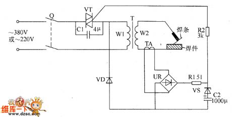
The welder no-load power saver circuit is composed of the current detection control circuit and power saving control circuit, and the circuit is shown as the chart. Current detection control circuit is composed of the current transformer TA, bridge rectifier UR, resistor R1, Zener diode VS, capacitor C2 and diode VD. Power control circuit consists of resistor R2, capacitor C1 and thyristor VT. R1 uses 3W wirewound resistor; R2 uses 2W metal film resistor. C1 uses the CBB capacitor or oil capacitor with the voltage being 630V; C2 uses the aluminium electrolytic capacitor with the voltage being 16V. VD selects 1N4007 silicon rectifier diode. VS selects 2CW12 silicon voltage regulator diode. UR selects 1A, 50V bridge rectifier.
(View)
View full Circuit Diagram | Comments | Reading(3691)
Welder no-load power saver circuit diagarm 4
Published:2011/6/10 4:22:00 Author:Lucas | Keyword: Welder, no-load , power saver
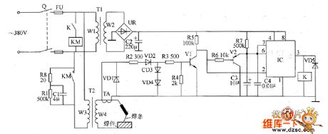
The welder no-load power saver circuit is composed of the +12 V power supply circuit, current detection control circuit, delay control circuit and the control implementation circuit, and the circuit is shown as the chart. +12 V power supply circuit is composed of the knife switch Q, fuse FU, power transformer T1, bridge rectifier UR and filter capacitor C2. Current detection control circuit is composed of the current transformer TA, diodes VD1 ~ VD4, resistors R2 ~ R6, transistors V1 and V2. Delay control circuit is composed of the resistor R7 and capacitors C3, C4, the time-base integrated circuit IC, relay K, AC contactor KM and diode VD5. R1, R3 ~ R7 select 1/4W metal film resistors; R2 uses 2W metal film resistor.
(View)
View full Circuit Diagram | Comments | Reading(797)
Welder no-load power saver circuit diagarm 3
Published:2011/6/10 6:06:00 Author:Lucas | Keyword: Welder, no-load , power saver

The welder no-load power saver circuit is composed of the power supply circuit, delay trigger circuit and the control implementation circuit, and the circuit is shown as the chart. Power supply circuit is composed of the knife switch Q, fuse FU, the normally open contact of AC contactor KM, welding transformer T, rectifier diode VD1, filter capacitor C2, Zener diode VS1 and current limiting resistor R1. The delay trigger circuit consists of Zener diodes VS2 and VS3, potentiometer RP, resistors R2 ~ R5, capacitor C3, diode VD2 and single-junction transistor VU. The control implementation circuit is composed of the relay K, diode VD3, thyristor VT, AC contactor KM and capacitor C1. R1 uses 1/2W metal film resistor; R2 ~ R5 select 1/4W metal film resistors.
(View)
View full Circuit Diagram | Comments | Reading(909)
Welder no-load power saver circuit diagarm 1
Published:2011/6/10 5:52:00 Author:Lucas | Keyword: Welder, no-load , power saver
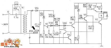
The welder no-load power saver circuit is composed of the relay drive circuit, low-voltage detection control circuit, high voltage time control circuit or voltage adaptive tracking regulation circuit, and the circuit is shown as the chart. The voltage adaptive tracking regulation circuit is composed of the voltage-regulator diode VS3, resistor R3 and transistors V3, V4. Relay driver circuit is composed of the relay K, transistors V1, V2 and diode VD3 and other components. KM is the AC contact, and C is the buck capacitor, K1 is the Κ normally open contact of the relay K, VD1 is the rectifier diode, C1 is the filter capacitor. R1 ~ R12 select 1W metal film resistors. C chooses non-polar condenser with the withstang voltage being 630V; C1 selects the aluminium electrolytic capacitor with the voltage being 250V.
(View)
View full Circuit Diagram | Comments | Reading(797)
555 household earthquake sound and light alarm circuit
Published:2011/6/2 19:10:00 Author:TaoXi | Keyword: 555, household, earthquake, sound, light, alarm circuit
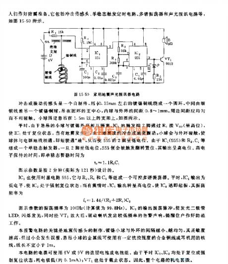
This circuit is composed of the impact sensor, the monostable trigger timing circuit, the multivibrator and the sound & light alarm circuit.etc, as the figure 15-50 shows.
The IC2 uses the time base circuit 555, the controllable multivibrator is composed of the IC2, R3, R4 and C3.etc, in peacetime the IC1 outputs the low electrical level to make the IC2 in the mandatory reset state; when the earthquake happens, the IC1 outputs the high electrical level to make the IC2 to start working, the oscillation frequency fc=1.44/(R3+2R4)C3.
The oscillation frequency of the figure parameters are 100Hz. IC2's output oscillation pulse makes the light-emitting diode LED1 to light, at the same time the pulse is amplified by VT1 to drive the speaker to send out the low-frequency alarm sound.
(View)
View full Circuit Diagram | Comments | Reading(926)
555 guest welcome and farewell electronic model circuit
Published:2011/6/7 8:26:00 Author:TaoXi | Keyword: 555, guest, welcome, farewell, electronic model
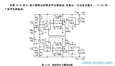
As the figure 15-35 shows, the electronic model is composed of two channels of generating circuit, each channel of circuit is composed of a photoelectric sensor, a 555 and a voice circuit.
The photoelectric sensor uses the 3DU type photosensitive tube, when the guest comes in or goes out, guest's body interrupts the light which illuminates on the VT1(or VT3), so the photosensitive tube has the high resistance, the pin-2's electric potential of 555 is lower than the 1/3VDD trigger electrical level, so the IC1 (or IC2) sets to output the high electrical level, the IC3 is triggered to send out the voice of welcome . At the same time the VT2 conducts, the collector electrode's low electric potential adds to the pin-4 of IC2 to mandatory reset the 555 no matter whether the VT3 has illumination.
(View)
View full Circuit Diagram | Comments | Reading(640)
Electronic detonating device circuit diagram 2
Published:2011/6/9 5:45:00 Author:Lucas | Keyword: Electronic, detonating device
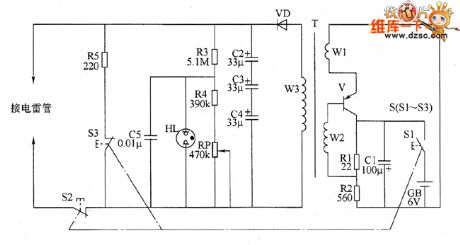
The electronic circuit is composed of the oscillator, booster circuit, charging instruction circuit and discharging circuit, and the circuit is shown as the chart. Oscillator circuit consists of transistor V, capacitor C1, resistor R1, R2, electric battery CB, charging switch S1 and the windings W1, W2 of step-up transformer T. The windings w3 of step-up transformer T, rectifier diode VD and capacitors C2 ~ C4. Charging instruction circuit consists of resistors R3, R4, potentiometer RP, capacitor C5 and neon light HL. Discharging circuit is composed of the discharging switch S2, discharging switch S3 and resistor R5. S1 ~ S3 is the three groups of control contacts of initiation button. R1 and R2 select 1/2W metal film resistors.
(View)
View full Circuit Diagram | Comments | Reading(657)
Electronic detonating device circuit diagram 1
Published:2011/6/9 5:37:00 Author:Lucas | Keyword: Electronic , detonating device
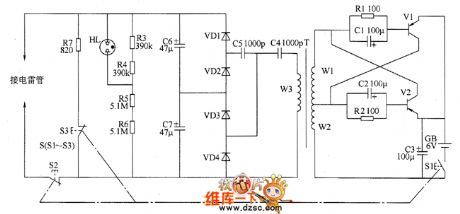
The electronic circuit is composed of the self-excited oscillator, high voltage generating circuit, charging instruction circuit and discharging circuit, and the circuit is shown as the chart. The self-excited oscillator circuit consists of resistors R1, R2, capacitors C1 ~ C3, transistors V1, V2, charging switch S1, battery CB, and the windings W1, W2 of step-up transformer T. The high-voltage generating circuit is composed of the winding W3 of step-up transformer T, capacitors C4 ~ C7 and rectifier diodes VD1 ~ VD4. C4, C5, and VD1 ~ VD4 form the doubler rectifier circuit. Charging instruction circuit consists of resistors R3 ~ R6 and neon light HL. Discharging circuit is composed of the discharging switch S2, bleed resistor R7 and bleed switch S3.
(View)
View full Circuit Diagram | Comments | Reading(605)
Welder no-load power saver circuit diagarm 12
Published:2011/6/10 4:14:00 Author:Lucas | Keyword: Welder , no-load , power saver

The welder no-load power saver circuit is composed of the current detection circuit, power supply circuit and switching control circuit and other components, and the circuit is shown as the chart. Current detection circuit is composed of the current transformer TA, rectifier diode VD5, transistor V2, potentiometers RP2 and related peripheral components. Power supply circuit is composed of the capacitor C5, power switch Q, signal transformer T1, rectifier diodes VD1 ~ VD4, VD6, VD7, Zener diode vs and filter capacitors C1 ~ C3 and other components. Switch control circuit consists of transistor V1, AC contactor KM and relay K and so on. R1 and R2 select 1W metal film resistors; R3 ~ R1O select 1W metal film resistors. RP1, RP2 select WH118 series of small synthetic carbon film potentiometer.
(View)
View full Circuit Diagram | Comments | Reading(1157)
Welder no-load power saver circuit diagarm 11
Published:2011/6/10 3:55:00 Author:Lucas | Keyword: Welder, no-load , power saver
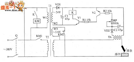
The welder no-load power saver circuit is composed of the knife switch Q, AC contactor KM, relay K, power transformer T1, welding transformer, transistors V1 and V2, resistors R1 and R2, capacitors C1 and C2, potentiometer RP, diodes VD1 and VD2 and current transformer TA, and the circuit is shown as the chart. In the circuit, T1, VD1 and C1 form the 24V DC power supply circuit; K, KM, R1, R2, RP, C2, VD2, and TA form the current detection and control circuit. R1 and R2 select 1/4W metal film resistors. RP uses solid organic or synthetic carbon film potentiometer; C1 and C2 select aluminium electrolytic capacitors with the voltage being 50V. VD1 and YD2 select lN4007 silicon rectifier diodes.
(View)
View full Circuit Diagram | Comments | Reading(1877)
KA2311 (toy) wireless remote control receiving control regulation circuit
Published:2011/6/1 9:39:00 Author:Lena | Keyword: wireless, remote control, receiving, regulation
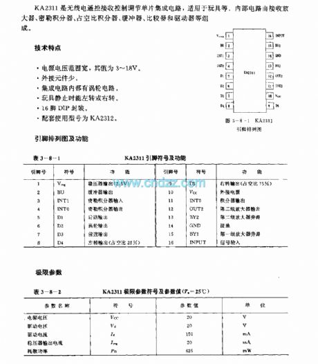
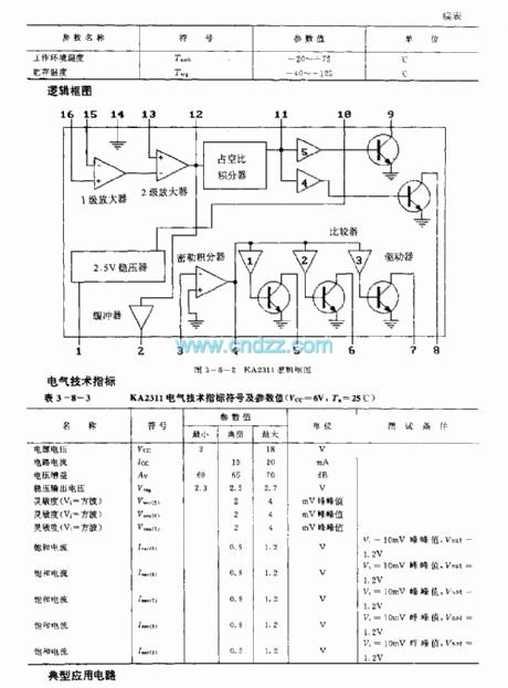
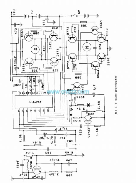
KA2311 is a wireless remote control receiving control regulation single integrated circuit which is applied to toys etc. Internal circuit consists of receiving amplifier, Miller integrator, duty cycle integrator, buffer, comparator and driver etc.
Technical characteristicWide power supply range, the value is 3-18V.Few external elements Integrated circuit with turbo circuitWhen the toy stops, it can turn left or right16-pin DIP packageRelated type is KA2312
(View)
View full Circuit Diagram | Comments | Reading(2355)
Current Detection Circuit Diagram made up of LM311 and Others
Published:2011/5/20 22:42:00 Author:leo | Keyword: Current Detection Circuit Diagram made up of LM311 and Others, LM311
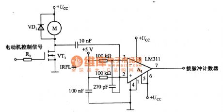
As what is shown in the picture, this is a current detection circuit diagram which is made up of LM311 and others. In this circuit, when the input control signal of the screen grid VT1 is in high level, it will use VT1 as the current detector. When the armature of DC electro-motor is turning, the commutator lug of brush shorts suddenly, which generates current pulses. The current pulses come through RDS of VT1 and are changed to voltage signals. Then the voltage signals are AC-coupled when passing through capacitor C1 and reach non inverting input port of comparison unit. C2 is used as filter which can make A1 output smooth wave shape that can be used in combination with pin 5 and pin6 to sharp the edge outputted by clock.
(View)
View full Circuit Diagram | Comments | Reading(1376)
KA2306A (toy)wireless remote control receiving control regulation circuit
Published:2011/6/1 9:11:00 Author:Lena | Keyword: wireless, remote control, receiving, regulation

KA2306A is a wireless remote control receiving control regulation single integrated circuit, applied to toys etc. Internal circuit consists of receiving amplifier, Miller integrator, buffer and voltage regulator etc.
Technical characteristicWide power supply range, the value is 3-18V.The current is small when at rest, the typical value is 10.5mAFew external elementsThe circuit has three functions, go ahead, stop and fall back.Integrated circuit has turbo circuit and voltage regulator served for super regenerative circuit.16-pin DIP package
(View)
View full Circuit Diagram | Comments | Reading(609)
KA2309(toy)wireless remote control receiving control regulation circuit
Published:2011/6/1 9:39:00 Author:Lena | Keyword: wireless, remote control, receiving, regulation
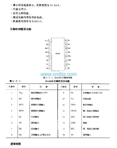
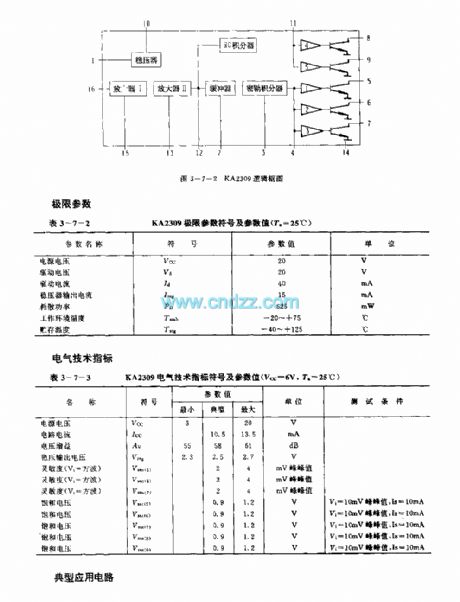
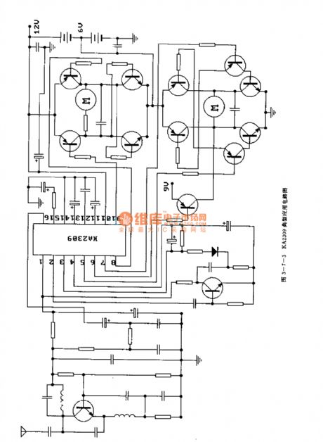
KA2309 is a wireless remote control receiving control regulation single integrated circuit applied to toys etc. Internal circuit consists of receiving amplifier, Miller integrator, RC integrator, buffer and voltage regulator etc.
Technical characteristicWide power supply range, the value is 3-18V.The current is small when at rest, the typical value is 10.5mAFew external elements Seven functions Integrated circuit with turbo circuitRelated type is KA2310
(View)
View full Circuit Diagram | Comments | Reading(2568)
WT-1 9823 Communication Single-Chip Microcomputer Integrated Circuit Diagram
Published:2011/5/20 19:14:00 Author:leo | Keyword: WT-1 9823 Communication Single-Chip Microcomputer Integrated Circuit Diagram
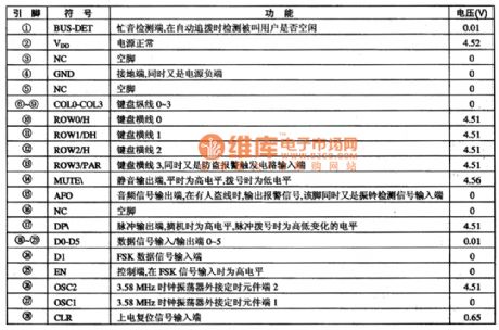
WT-1 9823 is a kind of single-chip microcomputer integrated circuit used for communication which is mainly applied in caller ID display telephone. The main feature of WT-1 9823 is that its integrated circuit contains pulse/dual-tone command circuit, FSK/DTMF caller ID display data processing circuit, clock circuit and input/output port, key switch coder-decoder circuit, silence control circuit, busy signal test circuit and so on. Its pins function and related data are as what is shown in the picture.
(View)
View full Circuit Diagram | Comments | Reading(665)
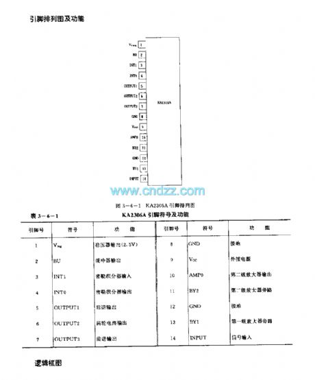
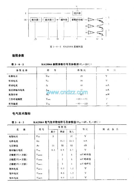
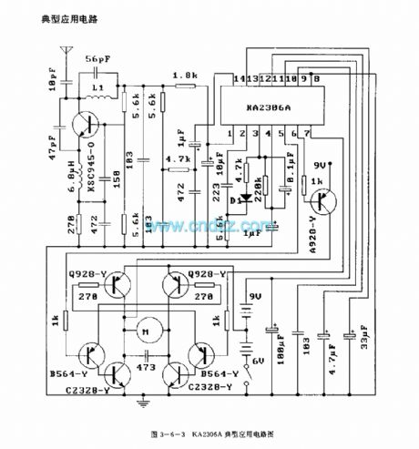
KA2305A (toy)wireless remote control receiving control regulation circuit
Published:2011/6/1 9:39:00 Author:Lena | Keyword: wireless, remote control, receiving, regulation
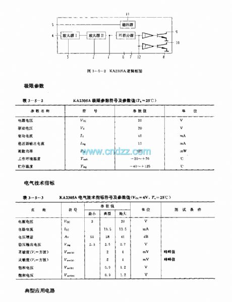
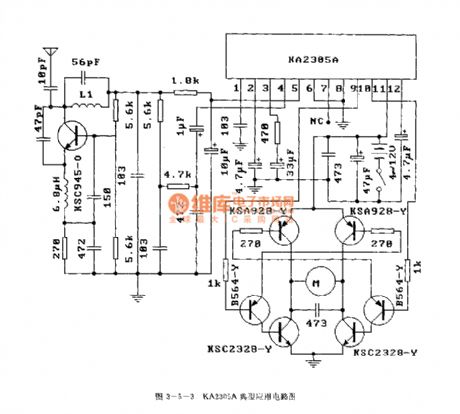
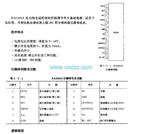
KA2305A is a wireless remote control receiving control regulation single integrated circuit applied to toys etc. Internal circuit consists of receiving amplifier, RC integrator, buffer and voltage regulator etc.
Technical characteristicWide power supply range, the value is 3-18V.The current is small when at rest, the typical value is 10.5mAFew external elementsThe circuit has three functions, go ahead, stop and fall back.12-pin SIP-SH package
(View)
View full Circuit Diagram | Comments | Reading(727)
| Pages:404/471 At 20401402403404405406407408409410411412413414415416417418419420Under 20 |
Circuit Categories
power supply circuit
Amplifier Circuit
Basic Circuit
LED and Light Circuit
Sensor Circuit
Signal Processing
Electrical Equipment Circuit
Control Circuit
Remote Control Circuit
A/D-D/A Converter Circuit
Audio Circuit
Measuring and Test Circuit
Communication Circuit
Computer-Related Circuit
555 Circuit
Automotive Circuit
Repairing Circuit