
power supply circuit
Index 143
8_A_positive_fixed-current_regulator_with_remote_sensing
Published:2009/7/23 23:56:00 Author:Jessie

This circuit uses the LAS3905 IC (Fig. 7-50) as a fixed current regulator with remote sensing. Characteristics are shown in Fig.7-50B, 7-50C, and 7-50D. (View)
View full Circuit Diagram | Comments | Reading(672)
Basic_F_V_converter_with_passive_filter
Published:2009/7/23 23:56:00 Author:Jessie
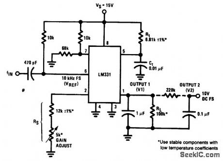
Fig. 12-21 This circuit is similar to that of Fig. 12-19, but with a passive filter added to reduce ripple. Typically, ripple is less than 1 mVp-p for frequencies from 200 Hz to 10 kHz. Again, set the 5-kΩ gain adjust for 10-V output with a 10-kHz input. National Semiconductor, Linear Applications Handbook 1991.p 1298. (View)
View full Circuit Diagram | Comments | Reading(730)
_5_V_500_mA_step_douon_converter_module
Published:2009/7/23 23:56:00 Author:Jessie
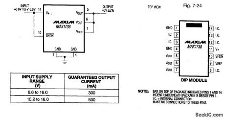
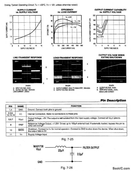
Figure 7-24 shows a MAX1738 2.5-W converter module that requires no extemal components. Figure 7-25 shows the pin descriptions and operating characteristics. The no-load current is 1.7 mA, with 60-μA shutdown current. Ripple is a typical ±30 mV, which can be improved using the optional output filter of Fig. 7-26. MAXIM NEW RELEASEs DATA BOOK, 1994, P. 4-23, 4-25, 4-26.
(View)
View full Circuit Diagram | Comments | Reading(659)
VOLTAGE_REGULATOR
Published:2009/7/3 2:10:00 Author:May
View full Circuit Diagram | Comments | Reading(0)
12_V_ynreset_output_high_efficiency_controller_non_boot_strayaped
Published:2009/7/24 3:14:00 Author:Jessie
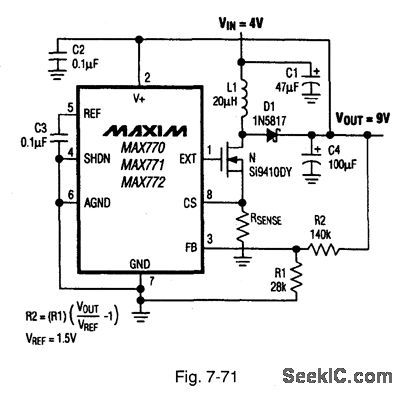
Figure 7-70 shows a MAX770/71/72 connected to provide 12-V output at 0.5 A, with a 5-V input. See Fig. 7-68 for component suppliers. This non-boot-strapped version of the Fig. 7-69 circuit requires less supply current, but with the full 5-V input. Use the Fig. 7-69 controller for input voltages less than 5 V. MAXIM NEW RELEASES DATA Book, 1995, P. 4-15. (View)
View full Circuit Diagram | Comments | Reading(606)
SCR_PREREGULATOR_FITS_ANY_POWER_SUPPLY
Published:2009/7/3 2:06:00 Author:May
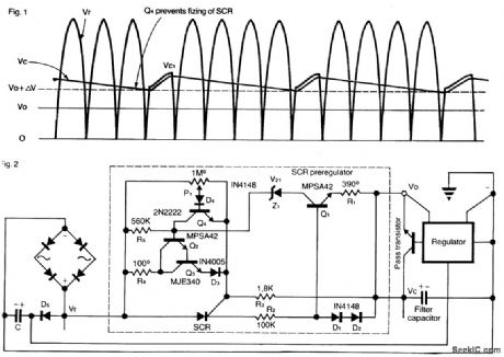
Circuit Notes
This SCR pre-regulator keeps the filter capacitor Vc, in a variable output power supply, a few volts above the output voltage Vo. The benefits include: less heat dissipated by the pass transistor and therefore small heatsink, cooler operation and higher efficiency, especially at low output voltages.Q1, R1, R2, D1 and D2 form a constant current source for zener Z1, so that the contribution to the output current is always a few mA (2-3 mA).The Darlington pair Q2, Q3 keeps the SCR off. The voltage Vcdecreases until Vc= Vo=V at which point the Darlington pair fires the SCR, charging the filter capacitor to a higher voltage Vc1 in less than half the period of the input voltage. The component values, shown are for a 0-250-V, 3-A power supply. (View)
View full Circuit Diagram | Comments | Reading(1)
Off_line_regulator_with_adjustable_output
Published:2009/7/24 0:07:00 Author:Jessie
In this circuit, the two regulators are connected in series to increase the voltage capability. However, neither regulator exceeds its maximum differential voltage-even under short-circuit conditions. (View)
View full Circuit Diagram | Comments | Reading(744)
3_A_positive_adjustable_voltage_regulator_1
Published:2009/7/24 0:06:00 Author:Jessie
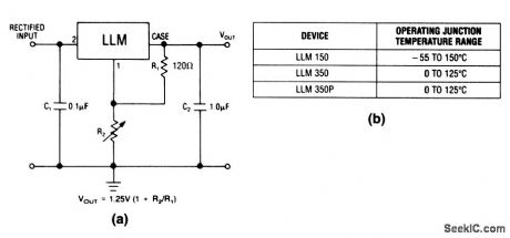
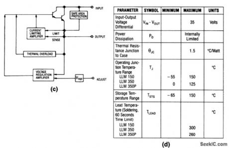
The LLM is a three-terminal adjustable regulator IC with an output range from +1.2 to +32 V, with the output voltage set by two external resistors. Because the regulator is floating, higher output voltages can be obtained as long as the maximum input-output differential is not exceeded. Characteristics are shown in Fig. 7-60B, 7-60C, and 7-60D. (View)
View full Circuit Diagram | Comments | Reading(806)
Three_terminal_regulator_for_high_voltages
Published:2009/7/24 0:13:00 Author:Jessie
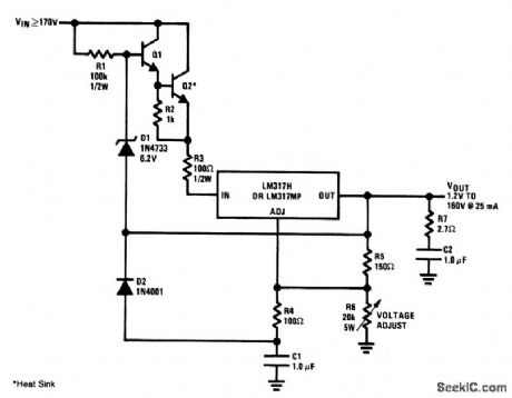
This circuit permits regulation of voltages well beyond the range or a three-terminal regulator. Notice that Q2 requires a heatsink because dissipation is 5 W for normal operation, and is possibly 10 W for a short circuit. (View)
View full Circuit Diagram | Comments | Reading(724)
Three_terminal_regulator_with_minimum_trimming
Published:2009/7/24 0:12:00 Author:Jessie
This circuit is similar to that of Fig. 7-64 and 7-65, but it should not require as much trimming. However, the tolerance is increased to 2%. (View)
View full Circuit Diagram | Comments | Reading(582)
Alternate_three_terminal_regulator_with_trimmable_output_voltage
Published:2009/7/24 0:11:00 Author:Jessie
This circuit is similar to that of Fig. 7-64, except that the resistors are shorted out initially with a jumper. The advantage of this circuit is that VOUT starts lower than the target value, and never exceeds that voltage during the trimming process. Follow the trimming (snipping) procedure shown. (View)
View full Circuit Diagram | Comments | Reading(693)
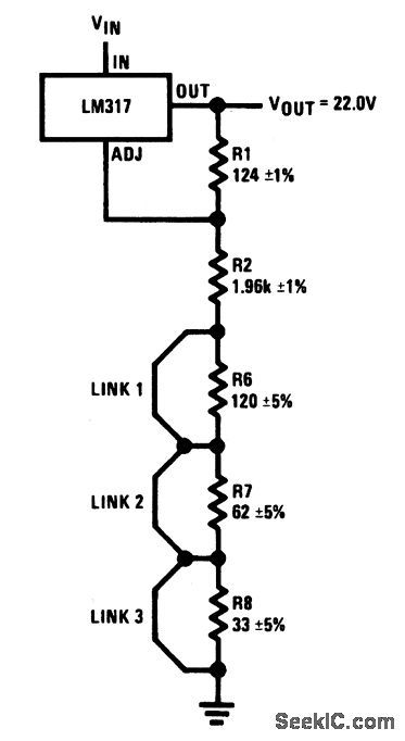
Three_terminal_regulator_with_trimmable_output_voltage
Published:2009/7/24 0:11:00 Author:Jessie
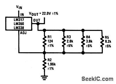
This circuit performs the same function of that shown in Fig. 7-63, except that a trim pot is not required (some engineers believe that good trim pots are expensive, inexpensive trim pots can be unreliable, and any trim pot that can be adjusted can also be misadjusted). When first tested, this circuit might have a VOUT 4% to 6% higher than the 22.0 V. While monitoring VOUT with a precision meter, snip out R3, R4, and/or R5, as necessary to bring VOUT within 1% of 22.0V. If VOUT is 23.08 V or higher, cut out R3 (if lower, do not cut R3). Then, if VOUT is 22.47 V or higher, cut out R4 (if lower, do not cut R4). Finally, if VOUT is 22.16 V or higher, cut out R5 (if lower, do not cut out R5). (View)
View full Circuit Diagram | Comments | Reading(721)
Three_terminal_regulator_with_small_adjustment_range_trim_pot
Published:2009/7/24 0:08:00 Author:Jessie

This circuit shows how a three-terminal regulator can be trimmed for a specific output voltage over a small range with a trim pot. (View)
View full Circuit Diagram | Comments | Reading(746)
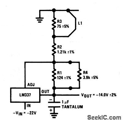
Extending_the_range_of_pnp_three_terminal_regulators
Published:2009/7/24 0:07:00 Author:Jessie

This circuit shows a way to extend the range of a pnp three-terminal regulator. The output voltage equals the regulator voltage plus the Zener voltage. If the Zener is selected to keep the input and ground-pin differential well below the IC breakdown, the input can exceed the maximum rating. For example, a 5-V three-terminal LM2931Z (maximum input 26 V) can become a 56-V regulator with a 51-V Zener. The input can be as low as 56.6 V with a load current of 150 mA or less. (View)
View full Circuit Diagram | Comments | Reading(956)
Regulated_voltage_up_converter
Published:2009/7/24 1:44:00 Author:Jessie
This circuit improves on the circuit of Fig. 8-7 in that the output remains within about 25 mV of 5 V for loads up to about 2 mA (still using two 1.5-V cells).Figure 8-7B also shows output voltage versus loading (shown as VOUT=5 V). (View)
View full Circuit Diagram | Comments | Reading(677)
Micropower_V_F_converter_10_kHz
Published:2009/7/24 1:43:00 Author:Jessie
Fig. 12-29 In this circuit, a 0- to 5-V input produces a 0 to 10-kHz output with a linearity of 0.02%. Drift is about 40 ppm/℃. Maximum current consumption is about 135μA-far below most IC V/F converters. To trim, apply 50 mV and select a value (typical 21 kΩ) at the C1 input for a 100-Hz output. Then, apply 5 V and adjust the 50-kΩ trim for a 10-kHz output. Linear Technology Linear Applications Handbook 1990 p AN23-11. (View)
View full Circuit Diagram | Comments | Reading(680)
FET_D_C_MILLIVOLTMETER
Published:2009/7/24 1:42:00 Author:Jessie
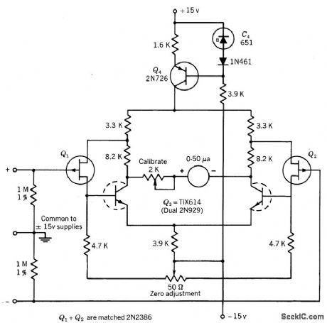
Uses differential amplifier assembled from pair of simple two stage feedback amplifiers having voltage gain of 3. Input sensitivity of meter is 20 meg per v and common mode rejection ratio is 1,000 to 1. Temperature characteristics are reasonably good when using matched let's.-Texas Instruments Inc., Transistor Circuit Design, McGraw-Hill, N.Y., 1963, p 522. (View)
View full Circuit Diagram | Comments | Reading(928)
MICROMODULE_FOR_16_MC_CLOCK_RAIE
Published:2009/7/24 1:42:00 Author:Jessie
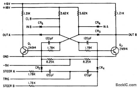
Flip-lop arrangement of two standard gales, with capacitor-resistor-diode gates fled to bases for trigger input, operates under worstcase temperature conditions with two standard gate loads.-A. S. Rettig, Computers in the Front Lines: Micromodules Make it Possible, Electronics, 36:1, p 77-81. (View)
View full Circuit Diagram | Comments | Reading(695)
Ultraprecision_V_F_converter
Published:2009/7/24 1:42:00 Author:Jessie
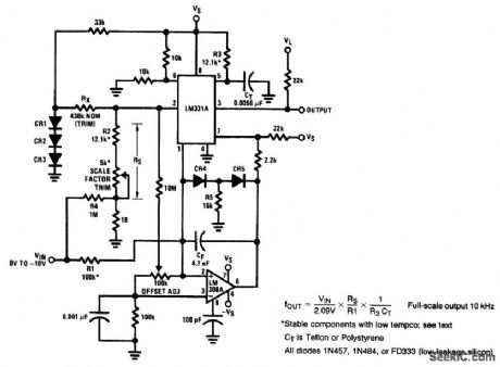
Fig. 12-28 This circuit is capable of better than 0.2% error and 0.003% nonlinearity for a ±20℃ range about room temperature. The basic V/F function of the LM331 is augmented by an LM308A connected as an integrator. To trim, connect the input to ground, and set the offset adjustment for zero output. Remove the ground and apply -10.000 V to the input and adjust the 5-kΩ scale factor trim for 10-kHz output. National Semiconductor Linear Applications Handbook, 1991 p. 1310. (View)
View full Circuit Diagram | Comments | Reading(1590)
_5_V_adjustable_inverting_PWM_regulators
Published:2009/7/24 1:37:00 Author:Jessie
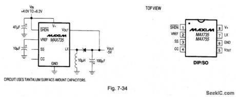
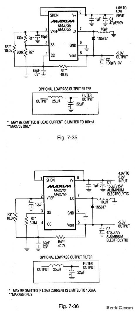
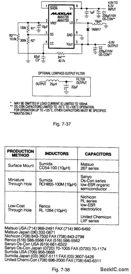
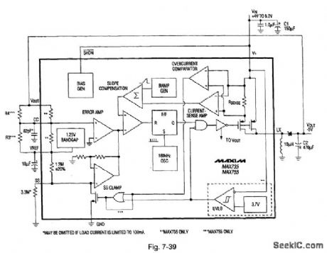
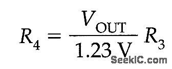
Figure 7-34 shows a MAX735 connected in a basic circuit to provide a 200-mA, -5-V output with a +4.0-V to +6.2-V input. Figure 7-35 shows the corresponding circuit using surface-mount components. Figure 7-36 shows the circuit using through-hole components (at commercial temperature ranges). Figure 7-37 shows the circuit using through-hole components (for all temperature ranges). Figure 7-38 shows component suppliers and Fig. 7-39 shows the block diagram with typical external components. The MAX755 operates from a +2.7-V to +9-V input and generates an adjustable negative output, depending qn the values of R3 and R4. The relationship is:Resistor R3 can be any value from 10 kΩ to 20 kΩ, VOUT is limited to 11.7 V -VIN. The quiescent current is 1.6 mA, with a 10-μA shutdown current. MAXIM NEW RELEASES DATA Book, 1994, P. 4-111, 4-115, 4-116, 4-117. (View)
View full Circuit Diagram | Comments | Reading(1007)
| Pages:143/291 At 20141142143144145146147148149150151152153154155156157158159160Under 20 |
Circuit Categories
power supply circuit
Amplifier Circuit
Basic Circuit
LED and Light Circuit
Sensor Circuit
Signal Processing
Electrical Equipment Circuit
Control Circuit
Remote Control Circuit
A/D-D/A Converter Circuit
Audio Circuit
Measuring and Test Circuit
Communication Circuit
Computer-Related Circuit
555 Circuit
Automotive Circuit
Repairing Circuit