
power supply circuit
Index 152
ANTIQUE_RADIO_POWER_SUPPLY
Published:2009/7/24 3:52:00 Author:Jessie
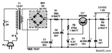
This supply was intended for powering an antique radio using 01A triodes needing dc filament voltage. It is a straightforward zener regulator and pass transistor. The large values or capacitance used are for reducing 120-Hz hum to a minimum. (View)
View full Circuit Diagram | Comments | Reading(902)
Low_voltage_single_cell_step_up_converter
Published:2009/7/24 3:52:00 Author:Jessie
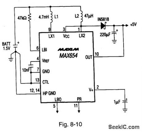
Figure 8-10 shows a MAX654 connected to provide a +5-V output at 40 mA with a 1.5-V input. The guaranteed start-up voltage is 1.15 V. The quiescent current shutdown is 80 μA. MAXIM HIGH RELIABILITY DATA Book, 1993, P. 4-37.
(View)
View full Circuit Diagram | Comments | Reading(641)
SMART_AC_POWER_STRIP
Published:2009/7/24 3:51:00 Author:Jessie
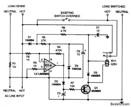
The schematic of the Smart Strip circuit is shown. The ac line input is connected directly to the 117-Vac line of a power strip. The voltage is rectified by diode D1 and filtered by capacitor C2. The load-sense lines are connected to the ac socket in the power strip that will contain the device that will be used to turn the others on. When the load sense device is turned on, current flows through R1, a 1-Ω, 10-W resistor. To limit the power in R1 to 5 W, therefore, amaximum load ofno more than 5 A should be connected to the load sense outlet. The resulting voltage drop across R1 is fed to one section of an LM358N op amp, IC1-a, through resistors R2 and R3. Zener diode D4 limits the supply for the op amp to 15 Vdc. The voltage drop across R1 could be very small if the device plugged into the load sense socket does not draw much current. To ensure that the circuit is sensitive enough to detect such small-load devices, the gain of IC1-a is set at 470 by resistors R2 and R4. Because the out-put IC1-a is halfway rectified, diode D2 and capacitor C3 are used to form a peak-hold circuit. As long as CB is charged to 0.7 V or more (when a powered-up load sense device is detected), transistor Q1 will be on, and relay RY1 will close. When those normally open contacts close, the hot line is connected to the load-switched sockets, effectively turning on any devices that are connected to those outlets. Diode D1, resistor R6, and capacitor C1 provide a dc supply for the 12-V coil of the relay; diode D3 acts as a clamping diode. (View)
View full Circuit Diagram | Comments | Reading(3428)
High_efficiency__5_V_step_dozon_regulator
Published:2009/7/24 3:50:00 Author:Jessie
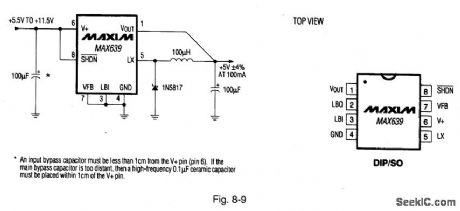
Figure 8-9 shows a MAX639 connected to provide +5-V output at 100 mA with inputs from +5.5 V to +11.5 V. Maximum quiescent current is 20 μA, with a typicai dropout of 0.5 V at (100-mA load). Efficiency is greater than 90%. MAXIM HIGH RELIAsILITY DATA BOOK, 1993, P. 4-31.
(View)
View full Circuit Diagram | Comments | Reading(610)
15__to_5_V_converter_with_800_μA_output
Published:2009/7/24 3:50:00 Author:Jessie
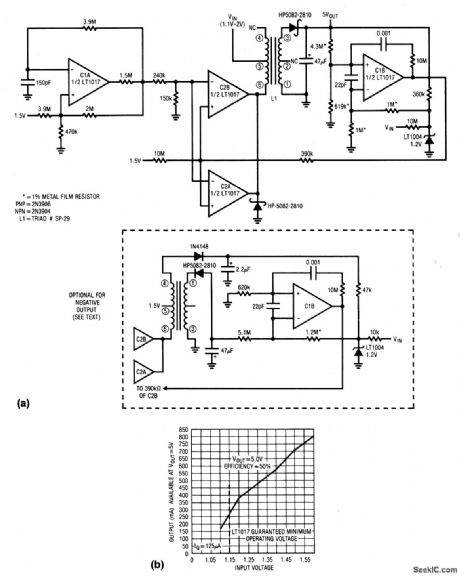
This circuit converts a single 1.5-V cell to a 5-V output with only 125 μA of quiescent current. Figure 8-47B shows a plot of output current versus input voltage. The optional connection (shown in dashed lines) uses the floating secondary of the transformer to produce a -5-V output. (View)
View full Circuit Diagram | Comments | Reading(874)
Correction_for_minimum_quiescent_current_near_dropout
Published:2009/7/24 3:48:00 Author:Jessie
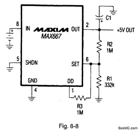
Figure 8-8 shows how the quiescent current or the MAX667 (Figs. 8-5, 8-6) can be further reduced near the dropout voltage (compared to the circuit of Fig. 8-7). MAXIM NEW RELEASES DATA Book, 1992, P. 4-138. (View)
View full Circuit Diagram | Comments | Reading(621)
OFF_LINE_REGULATOR
Published:2009/7/24 3:59:00 Author:Jessie
This circuit produces 8 to 12 Vdc using an off-line regulator. The ratio of the resistors determines the output voltage. The best value for R1 plus R2 is 250 kΩ, although the data sheet allows values between 200 and 300 kΩ. The 250-kΩ value minimizes loading, permitting the circuit to provide more accurate output voltage.WARNING: There is no isolation between line and load, and a potentially dangerous shock hazard exists. Do not use this circuit if the potential for accidental contact exists with the circuit and any other person or device. (View)
View full Circuit Diagram | Comments | Reading(846)
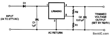
5_V_OFF_LINE_REGULATOR
Published:2009/7/24 3:58:00 Author:Jessie
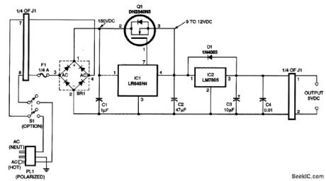
This circuit produces 5 Vdc using an off-line regulator. An input from 12 to 120 Vac is applied to pins 7 and 8 of the eight-pin circuit-board-mounted header (J1). Although the LR645N4 (IC1) accepts voltages up to 450 V, the input of this circuit is limited by the 200 PIV (peak inverse voltage) rating of the bridge rectifier (BR1). The full-wave-rectified input is applied to the 1-μF filter capacitor (C1). The filtered 150 Vdc is applied directly to pin 1 of IC1. Filter capacitance is unusually low because IC1 has a ripple rejection ratio (Vin/Vout) of 60 dB at 120 Hz with no load. The filtered input dc is also applied to pin 2 of the N-channel, depletion-mode MOSFET Q1, made by Supertex. It was designed to be compatible with LR6 linear regulators. MOSFET Q1 conducts up to 100 mA from the high-voltage source through the gate control line of the IC1, thus bypassing it. The combined regulated voltage and current source from Q1 and IC1 is then filtered through capacitor C2 to stabilize the regulated output. The regulated output of IC1 is applied to the LM340 (7805) voltage regulator (IC2) that regulates the output voltage of the combination of IC1 and Q1 to a logic-compatible 5 Vdc. The total available current at the 5-Vdc output is 100 mA, more than adequate current for most logic circuitry. The 5-Vdc is also filtered by 10-μF tantalum capacitor C3 for additional circuit stability under full current load.WARNING: There is no isolation between line and load, and a potentially dangerous shock hazard exists. Do not use this circuit if the potential for accidental contact exists with the circuit and any other person or device. (View)
View full Circuit Diagram | Comments | Reading(1606)
16__to_30_MHz_20_W_SSB_driver_136_V_supply
Published:2009/7/24 3:58:00 Author:Jessie
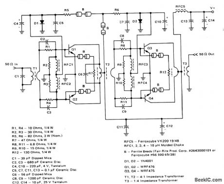
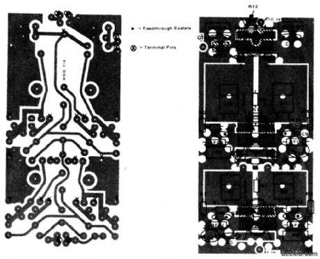
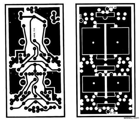
This amplifier provides a total power gain of about 25 dB, and uses inexpensive components (such as plastic RF transistors). The component layout, and PC-board layout, are shown in Figs. 2-55B and 2-55C, respectively. Both the parts and kits for this amplifier are available from: Communications Concepts, 121 Brown St., Dayton, Ohio 45402, (513) 220-9677. (View)
View full Circuit Diagram | Comments | Reading(960)
BATTERY_BACKUP_1
Published:2009/7/1 3:57:00 Author:May
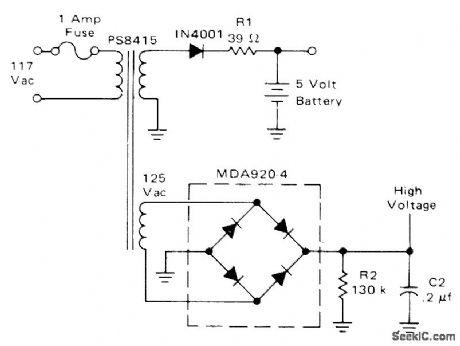
Four nickel-cadmium batteries connected in series provide automatic backup for 5-V supply of digital clock. Under normal AC line operation, battery is continually being recharged with half-wave rectified and unfiltered supply that allows internal chemical reactions to settle between pulses of charging energy. R1 is chosen to make average charging current about 5% of battery rating.-D. Ald-ridge and A. Mouton, Industrial Clock/Time( Featuring Back-Up Power Supply Operation, Motorola, Phoenix, AZ, 1974, AN-718A, p 7. (View)
View full Circuit Diagram | Comments | Reading(856)
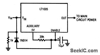
Basic_multifunction_regulcttor_application_computer_shutdown
Published:2009/7/24 3:57:00 Author:Jessie
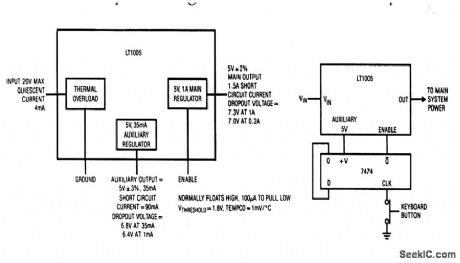
The LT1005 shown here is a multifunction regulator consisting of a 5-V 1-A regulator (controlled by a positive enable signal with a 1.6-V threshold) and a separate 5-V auxiliary regulator. The auxiliary regulator output is unaffected by the main regulator. The LT1005 also includes thermal overload protection and current limiting. The enable pin is a high impedance input which floats in the high state. 10 μA of current pulled from the enable pin shuts down the main output (but not the auxiliary). Figure 9-1B shows a simple, but useful, application. The enable pin is controlled by a toggling flip-flop triggered by a computer keyboard pushbutton. The auxiliary 5-V output powers the FF when the computer is shut down. This eliminates the need for a separate power switch. The enable pin interfaces directly with CMOS or TTL, but the relatively high impedance allows the pin to implement a number of other functions. (View)
View full Circuit Diagram | Comments | Reading(798)
Micropower_precision_reference
Published:2009/7/24 3:57:00 Author:Jessie
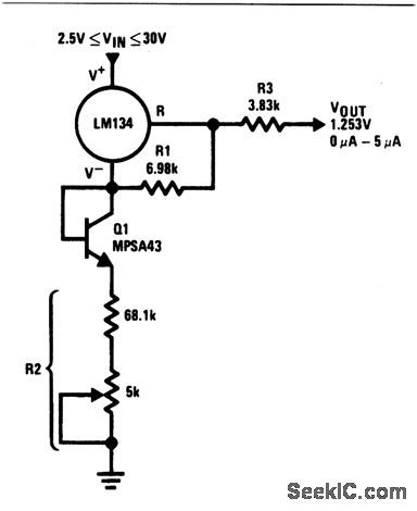
This circuit draws only 10 μA of current. The overall TC of the output will be near zero (less than 50 ppm/°C) when the output is adjusted to 1.253 V by trimming R2. R1 and R2 should track well over temperature. Metal-film resistors with 1% tolerance are recommended. (View)
View full Circuit Diagram | Comments | Reading(750)
Ultra_low_dropout_regulator
Published:2009/7/24 4:06:00 Author:Jessie
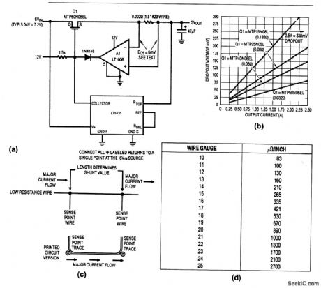
This simple regulator has only 85-mV dropout at 2.5 A. The low dropout makes the circuit particularly suitable for battery-driven laptop computers. The 12V required for the Q1 gate is found (on laptop computers) as the power source for disk drives and other peripherals. The shunt across the A1 inputs provides short-circuit protection. Figure 8-52C shows construction details for the shunt (both PC and wire versions). Figure 8-52D shows resistance versus size for various copper wire sizes. Figure 8-52B shows dropout characteristics for the circuit. (View)
View full Circuit Diagram | Comments | Reading(564)
Automatic_shutdown_for_load_shorts
Published:2009/7/24 4:05:00 Author:Jessie
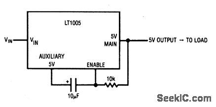
This circuit latches down the main regulator if a short occurs in the load. When power is applied, the auxiliary output comes up and transfers the charge through the capacitor. This forces the enable pin high, and allows the main regulator to come up and power the load. If a load short occurs, the regulator goes into current limit and the main output falls to zero. This pulls the enable pin low and completes a positive-feedback latch to disable the main output. Under these conditions, the output remains at zero-even after the load short is removed. Thus, the regulator need not dissipate power during the short. The output can be reset by removing the regulator input power (VIN) or by forcing the enable pin. (View)
View full Circuit Diagram | Comments | Reading(649)
Power_on_delay
Published:2009/7/24 4:04:00 Author:Jessie
When power is applied to this circuit, the output is held low until the capacitor charges beyond the 1.6-V threshold of the enable pin. With the RC values shown, the time required is about 100 ms. The diode/1-kΩ combination drains the capacitor quickly when power is removed. (View)
View full Circuit Diagram | Comments | Reading(928)
Precision_high_voltage_instrumentation_amplifier
Published:2009/7/24 4:04:00 Author:Jessie
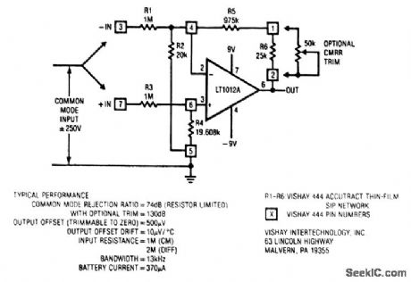
Although this circuit operates with two 9-V batteries, common-mode inputs of ±250 V are possible, with a voltage gain of 1. The circuit will also operate with ±15-V supplies, and with ±1.2-V supplies (with reduced common-mode range, of course). (View)
View full Circuit Diagram | Comments | Reading(808)
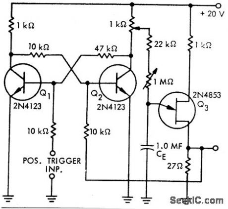
ASTABLE_MULTIVIBRATOR
Published:2009/7/1 2:51:00 Author:May
View full Circuit Diagram | Comments | Reading(0)
BATTERY_BACKUP
Published:2009/7/1 2:49:00 Author:May
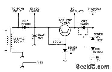
During normal operation, all power for dighal clock is provided by AC power supply. During power failure, clock con tinues operating from battery backup using two 9-V batteries in series. Battery drain is limited by diode CR2 that blocks power flow to displays. Optional switch may be installed across diode to short it for momentary viewing of display.-W. J. Prudhomme, CTT001 Clockbuster, 73 Magazine, Dec. 1976, p 52-54 and 56-58. (View)
View full Circuit Diagram | Comments | Reading(1073)
UJT_MONOSTABLE_CIRCUIT_INSESITIVE_TO_CHANGE_IN_BIAS_VOLTAGE
Published:2009/7/1 2:49:00 Author:May
View full Circuit Diagram | Comments | Reading(561)
Four_cell_NiCad_regulator_charger
Published:2009/7/24 4:11:00 Author:Jessie
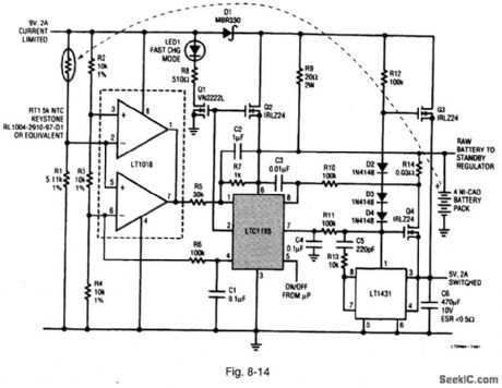
Figure 8-14 Shows an LTC1155 dual-power MOSFET driver connected to providecontrol of a four-cell charger/regulator. The LTC1155 has the ability to deliver 12-V of gate drive to two N-channel power MOSFETs when powered from a 5-V supplywith no external component required, The circuit is suited for a notebook-computer supply.(A four-cell NiCad battery pack can be used to power a 5-Vnotebook computer.)Q3 and Q4 must be provided with heatsinks.The regulator ISswitched off by the microprocessor when the battery voltage drops below 4.6V The standby current for the 5-V 2-A regulator is less than 10 μA.The regulator is switched on agam when the battery voltage rlses during charging. LINEAR TECHNOLOGY, DESIGN NOTE 51 P.1
(View)
View full Circuit Diagram | Comments | Reading(986)
| Pages:152/291 At 20141142143144145146147148149150151152153154155156157158159160Under 20 |
Circuit Categories
power supply circuit
Amplifier Circuit
Basic Circuit
LED and Light Circuit
Sensor Circuit
Signal Processing
Electrical Equipment Circuit
Control Circuit
Remote Control Circuit
A/D-D/A Converter Circuit
Audio Circuit
Measuring and Test Circuit
Communication Circuit
Computer-Related Circuit
555 Circuit
Automotive Circuit
Repairing Circuit