
power supply circuit
Index 151
10_W_CW_TRANSCEIVER_POWER_SUPPLY
Published:2009/7/24 3:34:00 Author:Jessie
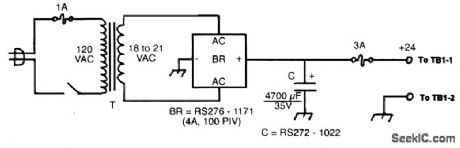
This power supply delivers about 24 Vdc at 1 A and was originally used for supplying power to a 10-W CW ham rig. (View)
View full Circuit Diagram | Comments | Reading(568)
Simple_nanometer_microammeter
Published:2009/7/24 3:33:00 Author:Jessie
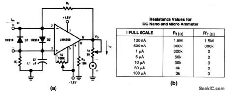
This circuit is an improved version of the circuit in Fig. 8-41, with diode input-overvoltage protection and meter-scale adjustments. Meter zero is set by R2, and full-scale deflection is set by R1 (typically, about 4 kΩ). Figure 8-41B shows the values of Rf for nanoammeter and microammeter operation. (View)
View full Circuit Diagram | Comments | Reading(2239)
12_DIGIT_GAS_DISCHARGE
Published:2009/7/1 20:21:00 Author:May
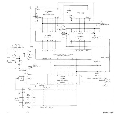
Display anodes are referenced to ground and cathodes to -180 V because number of digits in display is greater than number of segment drivers. Positive-logic CMOS address circuits are powered by -10 V, with Motorola MC14558 decoder outputs coupled to MC3491 segment drivers. Scan circuit is directly coupled to MC3490P anode drivers. Digit scanning is derived from two cascaded MC14022 octal counter/dividers. Required 12 sequenced output pulses are achieved by resetting counters with Q7 output of second counter. Counter output also controls system multiplexer (not shown) to give synchronization of entire display system.-A. Pshaenich, Interface Considerations for Numeric Display Systems, Motorola, Phoenix, AZ, 1975, AN-741, p 23. (View)
View full Circuit Diagram | Comments | Reading(1035)
LOW_STANDBY_POWER
Published:2009/7/1 20:20:00 Author:May
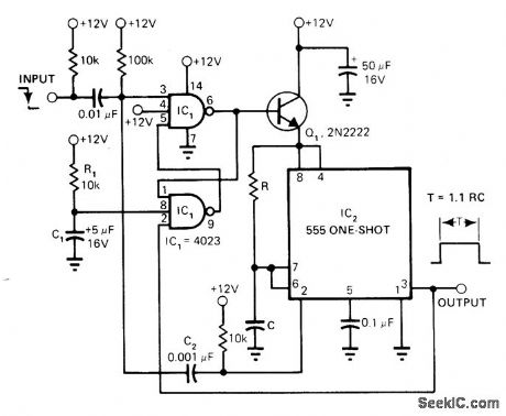
Basic 555 timer circuit is combined with control logic to keep drain from 12-V supply down to 1μA during standby. Drain increases to 6 mA when input signal makes output pulse go high. Circuit can be interfaced with CMOS logic. Negative-going input pulse triggers SR flip-flop, which in turn saturates a, and applies power to 555. Simultaneously, C2 feeds trigger to trigger input pin 2 of 555, to make output pulse go high. At end of time delay determined by values of R and C, timer output goes low and transition resets flip-flop for standby operation.-K. J. Imhof, 555 One-Shot Circuit Features Low-Power Standby Mode, EDN Magazine, April 20, 1978, p 134. (View)
View full Circuit Diagram | Comments | Reading(1484)
100_V_output_with_shunt_regulation
Published:2009/7/24 3:33:00 Author:Jessie
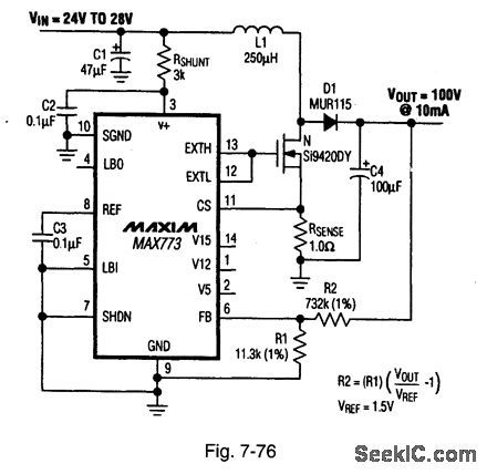
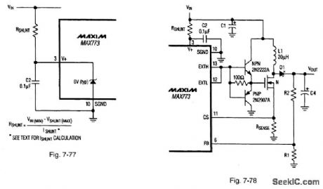
Figure 7-76 shows the MAX773 connected to provide 100-V output at 10 mA, with 24-V to 28-V input. Figure 7-77 shows the calculations for selecting the RSHUNT vaLue. RSHUNT should be selected so that ISHUNT is greater than 1 mA, but less than 20 mA. If the calculated shunt regulator current exceeds 20 mA, or if the shunt current exceeds 5 mA, and less shunt-regulator current is desired, use the circuit of Fig. 7-78. This provides increased drive and reduced shunt current when driving N-FETs with large gate capacitances. Use an ISHUNT of 3 mA. This provides adequate biasing current for the circuit, although higher shunt currents can be used. Notice that the shunt regulator is not disabled in the shutdown mode, and continues to draw the calculated shunt current. To prevent the shunt regulator from drawing current in the shutdown mode, place a switch in series with the shunt resistor.See Fig. 7-68 for component suppliers. MAXIM NEW RELEASES DATA Book, 1995, P. 4-152, 4-154.
(View)
View full Circuit Diagram | Comments | Reading(1031)
LOW_BATTERY_DRAIN
Published:2009/7/1 20:18:00 Author:May
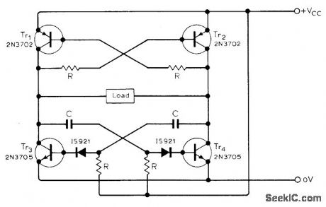
Combination of astable and bistable MVBRs, connected so diagonally opposite transistors switch on and off together, minimizes current drain in battery-powered signal generator. Period of square wave is approximately equal to 1.4CR, and peak load current can be up to 70 mA with 24-V battery supply. Circuit will tolerate wide range of values for CB.-J. C. Hopkins, Efficient Square-Wave Oscillator, Wireless World, June 1977, p 58. (View)
View full Circuit Diagram | Comments | Reading(801)
Micropower_voltage_reference
Published:2009/7/24 3:42:00 Author:Jessie
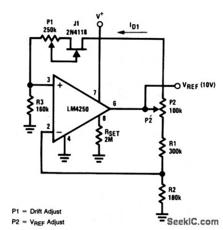
This circuit provides an adjustable voltage reference with a temperature coefficient of 0.002%/°C, and an overall standby current of less than 100 μA, using the zero-temperature-coefficient characteristic of a JFET (J1 is biased slightly below pinchoff by P1). (View)
View full Circuit Diagram | Comments | Reading(909)
Low_voltage_step_up_converter_with_higher_power_output
Published:2009/7/24 3:41:00 Author:Jessie
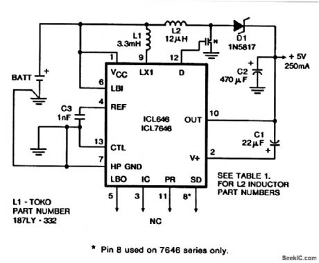
This circuit is similar to that of Fig. 8-42, except that an N-channel FET is added to provide 250 mA output current. (View)
View full Circuit Diagram | Comments | Reading(725)
Micropower_voltage_regulator
Published:2009/7/24 3:40:00 Author:Jessie
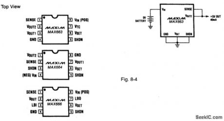
Figure 8-4 shows a MAX663 connected to provide a+5-V output at 40 mA from a 9-V battery. The maxlmum quiescent currentis 12 μA.MAXIM NEW RELEASES DATABook 1992. P.4-125. (View)
View full Circuit Diagram | Comments | Reading(794)
Quiescent_current_reduction_below_dropout
Published:2009/7/24 3:47:00 Author:Jessie
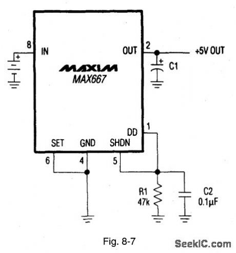
Figure 8-7 shows how the no-load quiescent current of the MAX667 (Figs. 8-5, 8-6) can be reduced to about 160 μA when the dropout voltage is reached. Notice that this circuit increases the dropout voltage by about 0.1 V MAXIM NEW RELEASES DATA BOOk, 1992, P. 4-138. (View)
View full Circuit Diagram | Comments | Reading(705)
Programmable_lozo_dropout_voltage_regulator
Published:2009/7/24 3:46:00 Author:Jessie
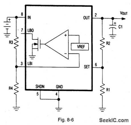
Figure 8-6 shows the MAX667 connected to provide a programmable output from +1.3 V to +16 V, with a low-battery function. Let R1 be 1 MΩ, and select R2 for a desired output using: R2= R1× (VOUT/VSET-1), where VSET= 1.225 V. Let R4 be 2.4 MΩ, and select R3 for a desired threshold of the low-battery detector using: R3=R4 ×(VBATT/VLBI-1). where VBATT is the desired threshold of the low-battery detector, and R3/R4 are the LBI input divider resistors. If VOUT is 5 V, a 5.5-V low-battery threshold can be set using 8.2 MΩ for R3 and 2.4 MΩ for R4. MAXIM NEW RELEASES DATA BOOk, 1992, p 4-137. (View)
View full Circuit Diagram | Comments | Reading(654)
Low_voltage_regulator
Published:2009/7/24 3:46:00 Author:Jessie
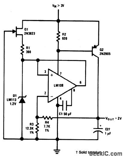
This circuit produces a 2-V output with a 3-V input. (View)
View full Circuit Diagram | Comments | Reading(752)
30_MHz_150_W_PEP_MOS_amplifier_28_V_supply
Published:2009/7/24 3:44:00 Author:Jessie
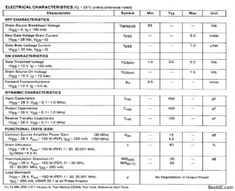
The electrical characteristics for the MRF140 shown in this circuit are given in Fig.2-52B (View)
View full Circuit Diagram | Comments | Reading(681)
Improved_micropower_voltage_reference
Published:2009/7/24 3:43:00 Author:Jessie
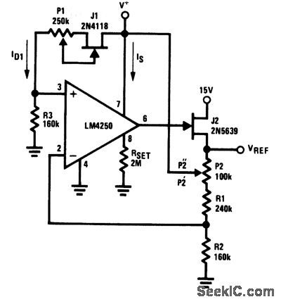
This circuit is an improved version of that shown in Fig. 8-44, but it requires an additional JFET to make the LM4250 independent of the unregulated input. (View)
View full Circuit Diagram | Comments | Reading(687)
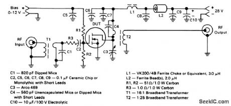
16_to_30_MHz_20_W_SSB_driver_28_V_supply
Published:2009/7/24 4:03:00 Author:Jessie
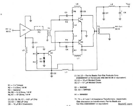
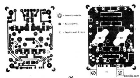
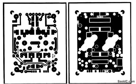
This amplifier provides a total power gain of about 55 dB, and is a 28-V vers1on of the circuit in Fig.2-55 The component layout,and PC-board layout, are shown in Figs.2-56B and 2-56C,respectively,Both the parts and kits for this amplifier are available from∶Communications concepts,121 Brown St, Dayton、Ohio45402(513)220-9677 (View)
View full Circuit Diagram | Comments | Reading(757)
DUAL_5_V_SUPPLY
Published:2009/7/24 4:02:00 Author:Jessie
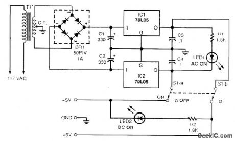
This is a circuit for a simple dual 5-V supply for experimental use. T1 is a 12-V center-tapped 0.3-A transformer. (View)
View full Circuit Diagram | Comments | Reading(796)
Flybctck_regulator_with_low_quiescent_current
Published:2009/7/24 4:02:00 Author:Jessie
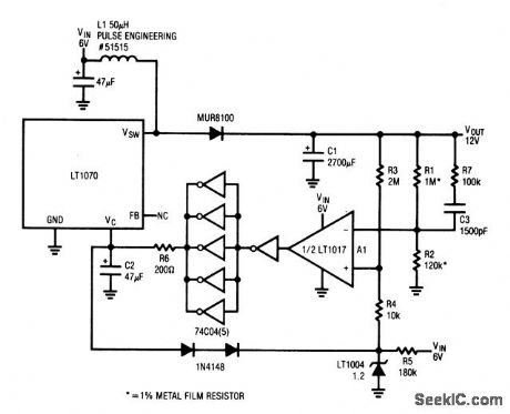
The quiescent current of this flyback regulator is a low 150 μA- even though the circuit is capable of delivery a maximum of 2 A at 12 V. (View)
View full Circuit Diagram | Comments | Reading(671)
15__to_5_V_converter_with_200_mA_output
Published:2009/7/24 3:56:00 Author:Jessie
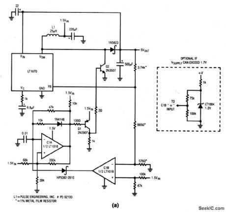
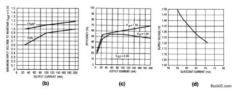
This circuit also converts 1.5 V to 5 V, but with higher output current and quiescent current than the circuit of Fig. 8-47. Figures 8-48B, 8-48C, and 8-48D show the characteristics. (View)
View full Circuit Diagram | Comments | Reading(717)
33_V_5_V_5_V_step_up_converter
Published:2009/7/24 3:54:00 Author:Jessie
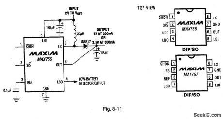
Figure 8-11 shows a MAX756 connected to provide a 5-V output at 200 mA or 3.3 V at 300 mA(depending on the status of 3/5 pm 2)with an input from 1.1 V to 5.5 V Quiescent current is 60 μA with a 20-μA shutdown current, and an efficiency of 87% (at 200 mA).MAXIM NEW RELEASES DATA Book 1994. P. 4-173.
(View)
View full Circuit Diagram | Comments | Reading(683)
IR_TRANSMITTER_POWER_SUPPLY
Published:2009/7/24 3:54:00 Author:Jessie
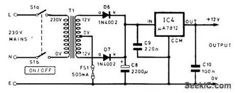
This supply provides 12 Vdc for an IR transmitter or other circuit. The current is about 260 mA. A 120-V transformer can be substituted for the 230-V unit shown, if desired. (View)
View full Circuit Diagram | Comments | Reading(585)
| Pages:151/291 At 20141142143144145146147148149150151152153154155156157158159160Under 20 |
Circuit Categories
power supply circuit
Amplifier Circuit
Basic Circuit
LED and Light Circuit
Sensor Circuit
Signal Processing
Electrical Equipment Circuit
Control Circuit
Remote Control Circuit
A/D-D/A Converter Circuit
Audio Circuit
Measuring and Test Circuit
Communication Circuit
Computer-Related Circuit
555 Circuit
Automotive Circuit
Repairing Circuit