
power supply circuit
Index 159
Positive_voltage_supply
Published:2009/7/24 21:24:00 Author:Jessie
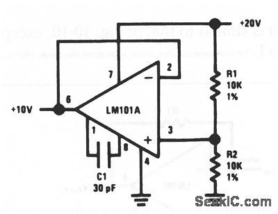
This circuit is designed specifically for the circuit of Fig. 10-13.However, this circuit can be used wherever a +10-V supply is needed. Notice that the output of this circuit is one-half the supply voltage because R1 and R2 are the same value. The same circuit can be used at other supply voltages, and with different ratios of R1 and R2. (View)
View full Circuit Diagram | Comments | Reading(965)
Op_amp_without_a_negative_supply
Published:2009/7/24 21:23:00 Author:Jessie
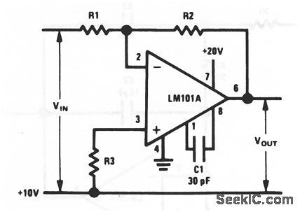
This circuit is similar to that of Fig. 10-2, except that a negative supply is not required. However, a second positive supply (+10 V) is required. The circuit of Fig. 10-14 can be used as the positive supply. (View)
View full Circuit Diagram | Comments | Reading(859)
Diode_bridge_based_rectifier_AC_voltmeter
Published:2009/7/24 20:38:00 Author:Jessie
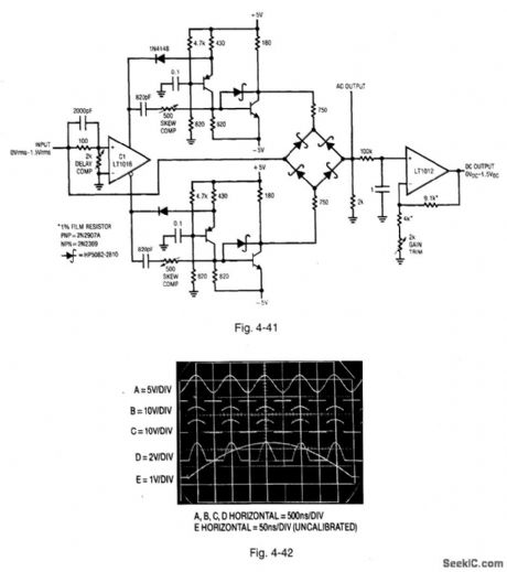
Figure 4-41 shows a circuit that provides both ac and dc outputs for inputs up to 2.5 MHz, Figure 4-42 shows the waveforms. Trace A shows the input sine wave. traces B and C are the switched corners of the bridge, trace D is the ac output, trace E is an expanded version of trace D, To calibrate, apply a 1-MHz to 2-MHz 1-V p-p sine wave and adjust the delay compensation so that bridge switching Occurs when the sine crosses zero. This adjustment corrects for the small delays through the LT1016 and the level shifters. Next, adjust the skew-compensation pots for minimum distortion in the ac output signal(trace D).These trims shift the phase of the rising output edge of their respective level shifter This allows skew in the complementary bridge-drive signals to be kept within 1 ns to 2 ns, minimizing output disturbances when switching Occurs. A 100-mV sine input will produce a clean output with a dc output accuracy of better than 0.25%,LINEAR TECHNOLOGY, APPLICATION Nom 43,P. 34. (View)
View full Circuit Diagram | Comments | Reading(1134)
Spike_suppressor_for_unregulated_power_supplies
Published:2009/7/24 13:56:00 Author:Jessie
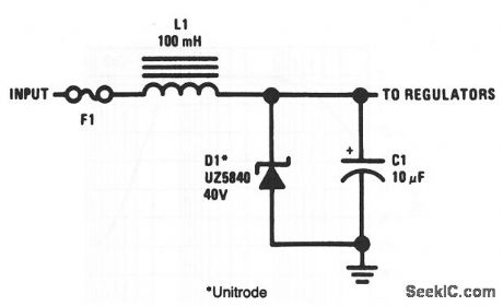
This circuit suppresses transients in unregulated supplies. Zener D1 clamps the input voltage to the regulator, and L1 limits the current through D1 during the transient. This circuit will clamp 70-V 4-ms transients. The value of L1=dVdt/I, where dV is the voltage by which the input transient exceeds the breakdown voltage of D1, dt is the duration of the transient, and I is the peak current of D1. National Semiconductor, Linear Applications Handbook, 1991, p. 47. (View)
View full Circuit Diagram | Comments | Reading(830)
CRO_HIGH_VOLTAGE_SUPPLY
Published:2009/6/30 2:11:00 Author:May
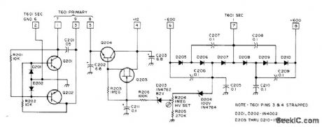
Controlled inverter operates from 12-V battery and feeds positive and negative triplers for producing ±600 V required for portable CRO, T601 high-voltage transformer has 22K,5.2K、and 600-ohm windings,all center-tapped,often marked Lionel when available in surplus shops,Q201,Q202、and Q204 are 2N697 or 2N2219,Q203 is 2N4302 or 2N5457.—G.E.Friton,Eyes for Your Shack,73 Magazine, Magazine,Nov./Dec,1975,p 74-76、78-88、and 90-94. (View)
View full Circuit Diagram | Comments | Reading(1762)
CRO_LOW_VOLTAGE_SUPPLY
Published:2009/6/30 2:07:00 Author:May
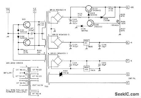
Developed for use as one of supplies for portable CR0, operating from battery using sealed rechargeable cells supplying 12 V at 2-5 Ah. High-efficiency inverter uses two GE D40C6 or RCA 2N5294 transistors (D101 and D102) as commutating switches for untapped feedback winding of power transformer. R102 then determines drive, while R101 produces required unbalanced starting bias. Thermistor R108 in series with CRT filament has cold resistance of 10 ohms to counteract very low cold resistance of CRT filament at start-up and prevent inverter malfunction. Article gives instructions for winding T101, along with high-voltage supply circuit and all other circuits of CRO covering DC to 10 MHz.—G. E. Friton, Eyes for Your Shack, 73 Magazine, Nov./Dee. 1975, p 74-76, 78-88 and 90-94. (View)
View full Circuit Diagram | Comments | Reading(1095)
Improved_5_V_power_supply_monitor
Published:2009/7/24 20:22:00 Author:Jessie
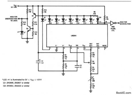
This circuit is an improved version of the circuit shown in Fig. 9-33. The calibration procedure is the same. (View)
View full Circuit Diagram | Comments | Reading(857)
5_V_power_supply_monitor
Published:2009/7/24 20:20:00 Author:Jessie
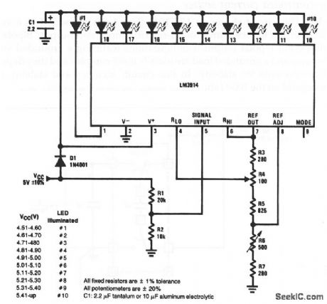
This circuit uses an LM3914 bar/dot display driver and 10 LEDs to form a simple power-supply monitor.To calibrate,set VCC at 5.41V and adjust R6 until LED9 and LED 10 are equally illuminated.Disconnect R1 from VCC,but leave D1 connected to VCC.Connect R1 to 4.500V,and adjust R4 until LED 1 just barely turns on.Readjust R6 and R1 as necessary. (View)
View full Circuit Diagram | Comments | Reading(819)
Precision_current_sensing_in_supply_rails
Published:2009/7/24 20:14:00 Author:Jessie
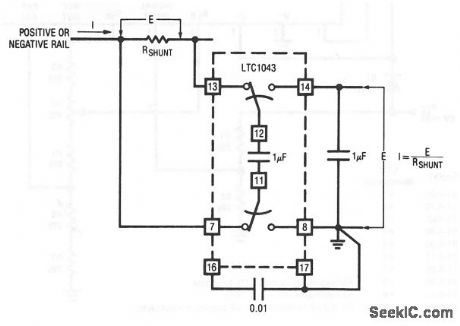
This circuit shows an LTC1043 (Fig. 1-4B) connected to sense current through a shunt in either of the supply rails. This capability has wide application in battery and solar-powered systems (chapter 8). If the ground-referred voltage output is unloaded by an amplifier, the shunt can operate with very little voltage drop across it, which minimizes losses. (View)
View full Circuit Diagram | Comments | Reading(728)
Voltage_controlled_current_source
Published:2009/7/24 20:14:00 Author:Jessie
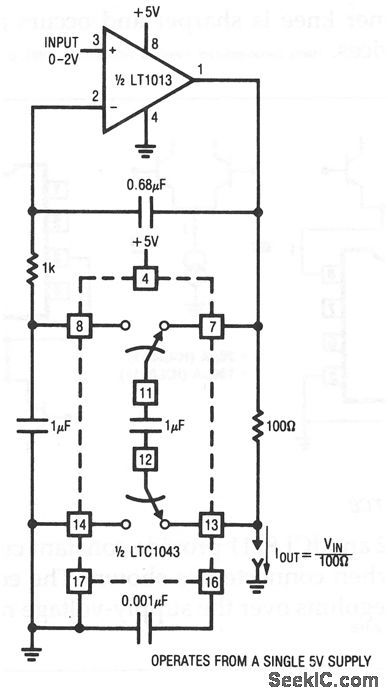
This circuit shows an LTC1043 (Fig. 1-4B) connected as a voltage-controlled current source with ground-referred input and output. Bipolar sup-plies will permit bipolar output. Configurations featuring a grounded voltage-control source and a grounded load are usually more complex and they depend on several components for stability. In this circuit, accuracy and stability almost entirely depend on the 100-Ω shunt. (View)
View full Circuit Diagram | Comments | Reading(0)
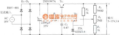
Step-down converting power circuit composed Of MC34063
Published:2011/5/5 20:03:00 Author:May | Keyword: Step-down, converting power
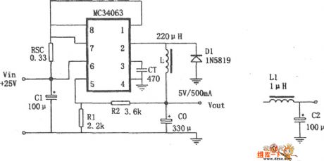
Step-down Vary Power Circuit Composed ofMC34063 is shown in the diagram. MC34063 is a type of switching modehighly active DC/DC Changed circuits. Its internalincludes reference voltage source withthe function of temperature compensation, comparator, duty ration controllable oscillator with limited current circuit, driver and heavy current output switch tube. The +25V/+5V step-down vary power composed of it is shown in the picture, the features are: (VIN=25V when IO=500mA) line regulation is 12mV±0.12%; load regulation is 3mV±0.03%; ripple voltage is 120mV. If one-level filter (shown in figure) output ripple reduced to 40mV; conversion efficiency is 82%; short-circuit limiting current is 1.1A.
(View)
View full Circuit Diagram | Comments | Reading(6546)
14_V_MAXIMUM
Published:2009/6/29 22:04:00 Author:May
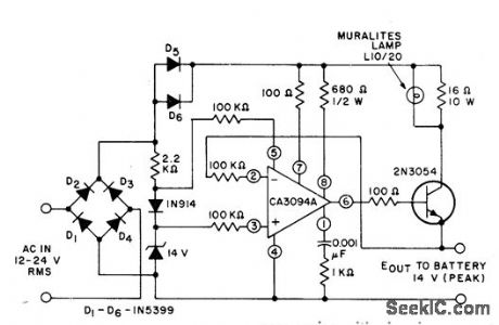
Circuit accurately limits peak output voltage to 14 V, as established by zener connected between terminals 3 and 4 of CA3094A programmable opamp. Lamp brightness varies with charging current. Reference voltage supply does not drain battery when power supply is disconnected.- Circuit Ideas for RCA Linear ICs, RCA Solid State Division, Somerville, NJ, 1977, p 19. (View)
View full Circuit Diagram | Comments | Reading(814)
Transistor regulator
Published:2011/7/23 10:39:00 Author:John | Keyword: Transistor regulator
View full Circuit Diagram | Comments | Reading(858)
Solar Garden Light
Published:2011/7/23 10:37:00 Author:John | Keyword: Solar Garden Light
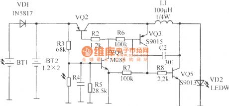
Solar garden light is as shown. When there is sunlight in the day, light energy is transferred into electrical energy by BT1. And BT2 charges the VD1. Due to the light, photosensitive resistor is with low resistance. VQ4 b closes due to very low electrical level. When there is no light at night, the photosensitive resistor is with high resistance. So VQ4 conducts. VQ2b also conducts due to very low electrical level. When the DC boost circuit composed of VQ3, VQ5, C2, R6 and L1 starts to work, LED powers to get light. The core of the DC boost circuit is a complementary tube oscillator circuit. (View)
View full Circuit Diagram | Comments | Reading(2042)
Common_mode_rejection
Published:2009/7/24 20:40:00 Author:Jessie
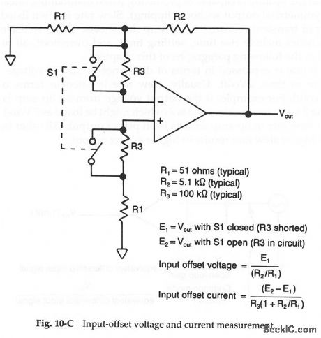
There are many definitions for common-mode rejection (CMR), also known as common-mode rejection ratio (CMRR). One definition is the ratio of differential gain (usually large) to common-mode gain (usually a fraction). That is, the amplifier might have a large gain of differential signals (different signals at each input terminal or with one input terminal grounded and the opposite input terminal with a signal), but little gain (or possibly a loss) of common-mode signals (same signal at both terminals). Another definition for CMR is the relationship of change in output voltage to change in input common-mode voltage producing the change, divided by the open-loop gain (amplifier gain without feedback).
No matter what definition is used, the first step to measure CMR is to find the open-loop gain of the IC at the desired operating frequency (chapter 1). Then, connect the IC in the common-mode circuit of Fig. 10-D. Increase common-mode voltage (at the same frequency used for the open-loop gain test) until a measurable output is obtained. Be careful not to exceed the maximum specified input common-mode voltage swing. If no such value is shown, do not exceed the normal input voltage of the IC. Then, find CMR using the equation.
To simplify the calculation, increase the input voltage until the output is 1 mV. With an open-loop gain of 100, this provides an equivalent differential input signal of 0.00001 V. Then, measure the input voltage. Move the input-voltage decimal point over five places to find CMR. (View)
View full Circuit Diagram | Comments | Reading(974)
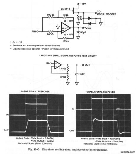
Dc_stabilization_with_differential_input_and_a_gain_of_1000
Published:2009/7/24 20:54:00 Author:Jessie
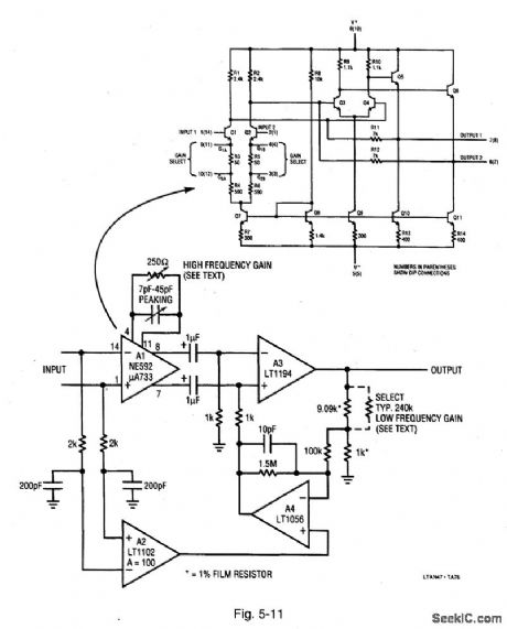
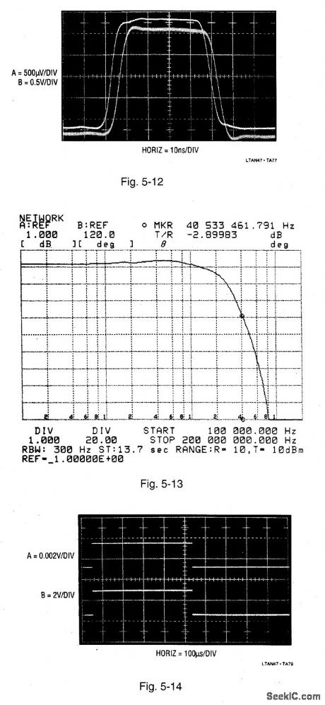
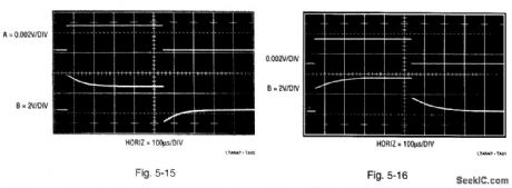
Figure 5-11 is similar to Fig. 5-9, but with a gain of 1000. The Fig. 5-11 circuit bandwidth is about 35 MHz, with full-power response available to 10 MHz. The rise time is 7 ns and delay is less than 7.5 ns. Input noise is about 15 μV broadband.Figure 5-12 shows the circuit response to a 60-ns, 2.5-mV pulse (trace A). The ×1000 output (trace B) has delay and rise times in the 5-ns to 7-ns range. Peaking can be trimmed with the adjustment at A1. Figure 5-13 plots the circuit gain versus frequency. Gain is flat within 0.5 dB to 20 MHz, with the -3-dB point at 38 MHz. The edge peaking shown in Fig. 5-12 shows up in Fig. 5-13 as a very slight gain increase, starting at about 1 MHz and continuing out to about 15 MHz. (This gain increase can be trimmed with the peaking adjustment, if necessary.) To use the circuit, apply a low-frequency or dc signal of known amplitude and adjust the low-frequency gain (parallel resistor) for a ×1000 output (after the output has settled). Next, adjust the high-frequency gain pot so that the output signal front and rear corners have amplitudes identical to the settled portion. Finally, trim the peaking-adjustment capacitor for best settling of the output pulse front and rear corners. Figure 5-14 shows the input (trace A) and output (trace B) waveforms with all adjustments properly set. Figure 5-15 shows the effects of too much ac gain (excessive peaking). figure 5-16 shows the effects of too much dc gain (long trailing response, with incorrect amplitude). LINEAR TECHNOLOGY, APPLICATION NOTE 47, P. 36, 37. (View)
View full Circuit Diagram | Comments | Reading(661)
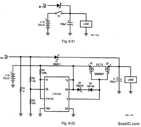
Switch_driver_for_18_V_to_28_V_operation
Published:2009/7/24 20:53:00 Author:Jessie
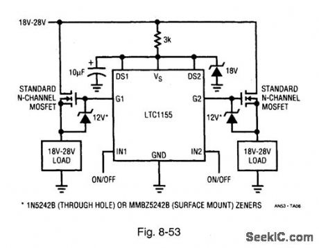
Figure 8-53 shows an LTC1155 connected for 18-V to 28-V switch-driver operation-even though the LTC1154/55/56 family is designed for 4.5-V to 18-V operation. The supply pin (Vs) is clamped to 18 V. These drivers typically produce 36-V of drive from a 18-V supply. This fully enhances N-channel MOSFET switches operating from 18 V to 28 V. The 12-V zener clamps are added to ensure that the maximum MOSFET VGS is not exceeded. LINEAR TECHNOLOGY, APPLICATION Note 53, P.4.
(View)
View full Circuit Diagram | Comments | Reading(703)
Bidirectional_MOSFET_switch_controllers
Published:2009/7/24 20:50:00 Author:Jessie
Figures 8-51 and 8-52 show manual and automatic bidirectional switches, respectively. Such circuits are used when the supply voltage is higher or lower than the load voltage, when powered by a secondary source. In the manual circuit of Fig. 8-51, 51 disconnects the battery from both the load and source when VIN (from a wall-unit power supply) is connected. This permits the load voltage to fluctuate above or below the battery voltage, without forcing current into (or out of) the battery. In the far more practical automatic circuit of Fig. 8-52, Q1 and Q2 fully disconnect the battery from the load immediately after the wall-unit supply is connected to VIN. The two diodes in Q1 and Q2 are also connected back to back, and no current can flow through the switch when the gate drive is removed. The LTC1154 EN (enable) input senses when the wall-unit voltage exceeds 3 V, and inverts the switch action so that Q1/Q2 are turned off when the wall-unit supply is disconnected. LINEAR TECHNOLOGY, APPLICATION NOTE 53, P. 3.
(View)
View full Circuit Diagram | Comments | Reading(2069)
Op_amp_troubleshooting
Published:2009/7/24 20:50:00 Author:Jessie
The troubleshooting approach described for the amplifiers of chapter 1 can be applied to op-amp circuits of this chapter. That is, first test the circuit to see if it performs the desired function, If not, try correcting the problem with adjustments. Then, trace signals using a meter or scope from input to output. If any portion of the circuit has a normal input, and an abnormal output, you have located the area in which the trouble occurs. From that point on, it is a matter of voltage measurements and/or point-to-point resistance measurements. The following are a few examples.
In the circuit of Fig. 10-19, there should be a TTL-level output for a small differential input voltage. For example, if you ground one input, and apply a signal to the opposite input, there should be a TTL-level output at pin 6. If you ground both inputs, there should be no signal output. However, the output might shift in voltage level because of the input-offset voltage.
If there is no output with a differential-signal input, suspect the LM101A. If there is an output from the LM101A, but not at the desired TTL level, suspect the LM103.
In the circuit of Fig. 10-20, there should be an output when the photodiode is exposed to light. Because it is difficult to monitor the input current, measure the voltage across R2 (from pin to ground). If there is no change in output voltage when the photodiode is exposed to varying light conditions, suspect the photo-diode, the LM101A, or D2. If the output does change with light current, check the values of R1, R2, and D2. It is also possible that the photodiode is defective, and producing a nonlinear output. (View)
View full Circuit Diagram | Comments | Reading(976)
Dc_stabilization_with_high_input_impedance_
Published:2009/7/24 20:45:00 Author:Jessie
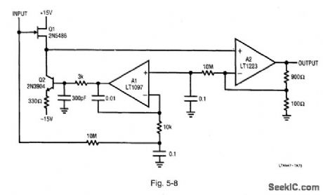
Figure 5-8 shows a dc-stabilized, wideband amplifier using a FET input for high input impedance. Input capacitance is about 3 pF, the bandwidth is 100 MHz, and the gain is 10 (using the feedback values shown). A1 stabilizes the circuit by controlling the Q1 channel current through feedback. LINEAR TECHNOLOGY, APPLICATION NOTE 47, P. 34. (View)
View full Circuit Diagram | Comments | Reading(848)
| Pages:159/291 At 20141142143144145146147148149150151152153154155156157158159160Under 20 |
Circuit Categories
power supply circuit
Amplifier Circuit
Basic Circuit
LED and Light Circuit
Sensor Circuit
Signal Processing
Electrical Equipment Circuit
Control Circuit
Remote Control Circuit
A/D-D/A Converter Circuit
Audio Circuit
Measuring and Test Circuit
Communication Circuit
Computer-Related Circuit
555 Circuit
Automotive Circuit
Repairing Circuit