
power supply circuit
Index 147
Voltage_boosted_output_op_amp
Published:2009/7/24 2:03:00 Author:Jessie
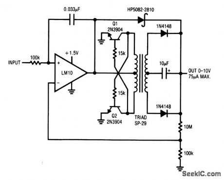
This 1.5-V powered amplifier provides 0 to 10 V outputs at up to 75-μA capacity. With the values shown, voltage gain is about 100. Gain can be increased provided that the 1.5-V powered LM10 common-mode input not be exceeded. (View)
View full Circuit Diagram | Comments | Reading(686)
GO_NO_GO_VTVM
Published:2009/7/24 2:03:00 Author:Jessie
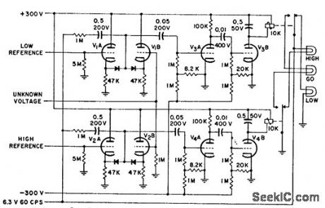
For applications in which voltage with specified tolerance must be monitored by unskilled production-line personnel. Three lamps indicate voltage. Go band can be as narrow as 0.1 v. Basic range of 100 v can be extended with dividers.-A Go No-Go Vacuum Tube Voltmeter, Electronic Circuit Design Handbook, Mactier Pub. Corp., N.Y., 1965, p 156. (View)
View full Circuit Diagram | Comments | Reading(716)
PHOTOCELL_CHOPPER
Published:2009/7/24 2:02:00 Author:Jessie
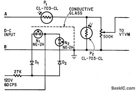
Allows millivolt d-c voltages to be measured accurately with ordinary average-reading vtvm. Neon lamps are fired alternately by rectified 60-cps line voltage, causing Clairex photocells to alternate between low und high resistance states and thereby chop d-c input voltage being measured.-I. Queen, Chopper Adapts Voltmeter to D-C, Electronics, 38:22, p 66-67. (View)
View full Circuit Diagram | Comments | Reading(913)
2_A_5_A_step_doryn_PWM_regulators
Published:2009/7/24 2:02:00 Author:Jessie
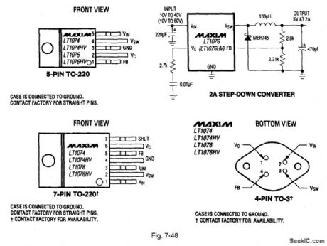
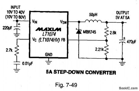
Figure 7-48 shows an LT1076 connected to provide an output of +5 V at 2 A, with an input of 10 V to 40 V. Figure 7-49 shows an LT1074 connected to provide an output of +5 V at 5 A, with an input of 10 V to 40 V. Both ICs have a quiescent current of 8.5 mA. MAXIM NEW RELEASES DATA BOOK, 1994, P. 4-251, 4-254. (View)
View full Circuit Diagram | Comments | Reading(1633)
BALANCED_VTVM
Published:2009/7/24 2:01:00 Author:Jessie
V1 operates at low plate current to keep grid current small; V2 operates normally to drive meter circuit. R1 is switched for voltage ranges. Chief drawback is that aging of tubes increases their output resistances, making meter read low.-J. J. Faran Jr., Hybrid Voltmeter Avoids Aging Errors, Electronics, 36:38, p 41. (View)
View full Circuit Diagram | Comments | Reading(792)
Micropower_switching_regulator
Published:2009/7/24 2:18:00 Author:Jessie

This circuit operates from a 6- or 9-V battery and provides 5-V output at 20 mA. Figure 8-18B shows output current and efficiency for both 6- and 9-V operation. (View)
View full Circuit Diagram | Comments | Reading(775)
Single_cell_sample_hold
Published:2009/7/24 2:14:00 Author:Jessie
This 1.5-V powered sample-hold circuit has an acquisition time of 125 μS to 0.1% with a droop rate of 10 μV/ms. Current consumption is less than 700 μA. (View)
View full Circuit Diagram | Comments | Reading(803)
12_V_high_efficiency_controller_non_boot_stmpped
Published:2009/7/24 2:13:00 Author:Jessie
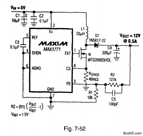
Figure 7-52 shows the MAX1771 connected to provide 12-V output at 0.5 A, with a 5-V input. See Fig. 7-51 for component suppliers. This non-boot-strapped version of the Fig. 7-50 controller requires less supply current, but with the full 5-V input. Use the Fig. 7-50 controller for input less than 5 V. Maxnvt NEW RELEASES DATA BOOK, 1995, P. 4-20.
(View)
View full Circuit Diagram | Comments | Reading(788)
MEASURING_SPOT_WELDING_CURRENT
Published:2009/7/24 2:08:00 Author:Jessie

Toroid placed around one of welder electrodes develops voltage that is function of rate of change of magnetic flux produced by alternating current lowing through weld. Peak-reading a-c electronic voltmeter is used to measure resulting voltage across toroid. Selector switch positions are: 1-no signal input; 2-0 to 15,000 amp; 3-0 to 30,000 amp; 4-calibration.-J. Markus, Handbook of Electronic Control Circuits, McGraw-Hill,1959, p 326. (View)
View full Circuit Diagram | Comments | Reading(1179)
PRESET_VOLTAGE_LIMIT_MONITOR
Published:2009/7/24 2:07:00 Author:Jessie
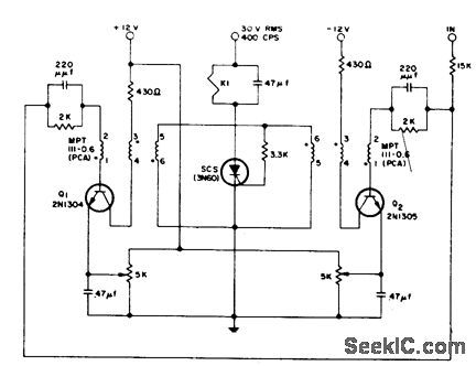
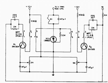
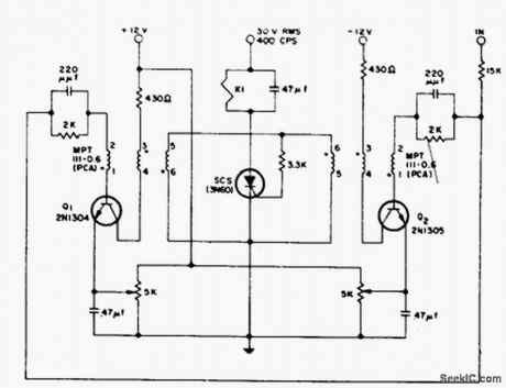
Used In automatic testing equipment to determine if voltage is within required go-band, Uses complementary transistors In blocking oscillator circuits with high Input impedance and with low hysteresis at switching limits.-L. Smith, High-Impedance Voltage Monitoring Circuit, EEE, 12:4,p 65. (View)
View full Circuit Diagram | Comments | Reading(847)
A_C_OPERATED_PEAK_READING_VOITMETER
Published:2009/7/24 2:06:00 Author:Jessie
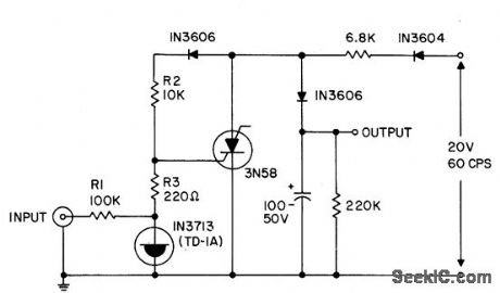
Uses tunnel diode and silicon controlled switch to give d-c output proportional to positive peak of input signal- Transistor Manual, Seventh Edition, General Electric Co., 1964, p 371. (View)
View full Circuit Diagram | Comments | Reading(619)
Single_cell_flyback_regulator
Published:2009/7/24 2:05:00 Author:Jessie
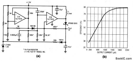
This 1.5-V powered regulator provides a 5-V output, at currents up to 2200 μA. As shown by the graph of Fig. 8-14B, efficiency is greatest at currents above 1500 μA, and drops off at lower currents (because of fixed losses in the regulator). (View)
View full Circuit Diagram | Comments | Reading(697)
9_V_high_efficiency_controller
Published:2009/7/24 2:17:00 Author:Jessie
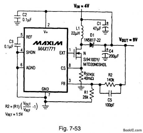
Figure 7-53 shows the MAX1771 connected to provide 9-V output with a 4-V input. See Fig. 7-51 for component suppliers.AXIM NEW RELEASES DATA BOOk, 1995.P4-20. (View)
View full Circuit Diagram | Comments | Reading(742)
Micropower_sample_hold
Published:2009/7/24 2:17:00 Author:Jessie
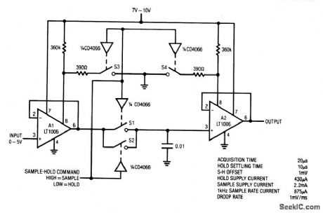
This sample-hold circuit has an acquisition time of 20 μS, with a hold-current of 430 μA, and a sample-current of 2.2 mA. (View)
View full Circuit Diagram | Comments | Reading(734)
DC_TO_DC_SMPS_VARIABLE_18_V_TO_30_V_OUT_AT_02_A
Published:2009/7/2 5:29:00 Author:May
View full Circuit Diagram | Comments | Reading(683)
PULSE_WIDTH_DETECTOR
Published:2009/7/2 5:27:00 Author:May

Logic terminal of National LM122 timer is driven simultaneously with trigger input to give high-accuracy pulsewidth detector. Output changes state onlv when trigger input stays high for longer than time period set by Rt and Ct; resulting output pulse width is then equal to input trigger width minus RtCt. CL filters out narrow spikes that would occur at output due to interval delays during switching. Supply can range from 4.5 to 4O V.-C. Nelson, Versatile Timer Operates from Microseconds to Hours, National Semi-conductor, Santa Clara, CA, 1973, AN-97, p 9. (View)
View full Circuit Diagram | Comments | Reading(3215)
12_14_V_REGULATED_3_A_POWER_SUPPLY
Published:2009/7/2 5:27:00 Author:May
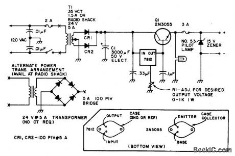
View full Circuit Diagram | Comments | Reading(740)
LOW_LEVEL_ACTIVATION_BY_CMOS
Published:2009/7/2 5:23:00 Author:May
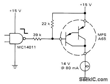
Typical CMOS gate interf aces directly with small-signal Darlington transistor driving 80-mA lamp load.-A. Pshaenich, Interface Techniques Between industrial Logie and Power Devices, Motorola, Phoenix, AZ, 1975, AN-712A, p 11. (View)
View full Circuit Diagram | Comments | Reading(761)
90_V_rms_VOLTAGE_REGULATOR_USING_A_PUT
Published:2009/7/2 5:23:00 Author:May
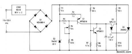
Circuit Notes
The circuit is an open loop rms voltage regulator that will provide 500 watts of power at 90 V rms with good regulation for an input voltage range of 110-130 V rms. With the input voltage applied, capacitor C1 charges until the firing point of Q3 is reached causing it to fire. This turns Q5 on which allows current to flow through the load. As the input voltage increases, the voltage across RIO increases which increases the firing point of Q3. This delays the firing of Q3 because C1 now has to charge to a higher volt-age before the peak-point voltage is reached. Thus the output voltage is held fairly con-stant by delaying the firing of Q5 as the input voltage increases. For a decrease in the input voltage, the reverse occurs. (View)
View full Circuit Diagram | Comments | Reading(1041)
Regulator_with_logic_output_on_dropout_battery_low
Published:2009/7/24 2:21:00 Author:Jessie
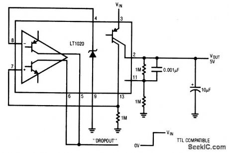
This circuit produces a logic-1 output when the regulator begins to drop out (battery low). The logic-1 signal can be used to alert a processor (or similar circuit) that power is about to go down. (View)
View full Circuit Diagram | Comments | Reading(752)
| Pages:147/291 At 20141142143144145146147148149150151152153154155156157158159160Under 20 |
Circuit Categories
power supply circuit
Amplifier Circuit
Basic Circuit
LED and Light Circuit
Sensor Circuit
Signal Processing
Electrical Equipment Circuit
Control Circuit
Remote Control Circuit
A/D-D/A Converter Circuit
Audio Circuit
Measuring and Test Circuit
Communication Circuit
Computer-Related Circuit
555 Circuit
Automotive Circuit
Repairing Circuit