
power supply circuit
Index 154
Nonvolatile_power_supply_malfunction_detector
Published:2009/7/24 5:19:00 Author:Jessie
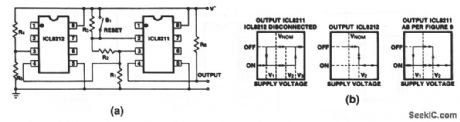
This circuit detects and stores the fact that an out-of-operating-range supply-voltage condition has occurred-even when the supply drops to 0. The circuit works on both high and low supply malfunctions so that the circuit can detect when a low supply voltage might have caused a volatile memory loss, or when an overvoltage might have damaged components, or any similar transient/intermittent power failure. The circuit operates with any supply range between 2 and 30 V. Figure 9-23B shows the output states as a function of supply voltage.Figure 9-21B shows the equations to calculate resistor values. The ICL8212 detects voltage V2, which is the upper limit of the operating voltage range. The ICL8211 detects the lower voltage limit of range V1. Hysteresis is used with the ICL8211 so that the output can be stable in either state over the operating voltage range from V1 to V2 by making V3 (the upper trip point of the ICL8211) much higher in voltage than V2. The ICL8212 output forces the ICL8211 output into the on-state above V2 Thus, there is no value of supply voltage that will result in the output of ICL8211 charging from the on-state to the off-state. This can be achieved only by shorting out R3 for values of supply voltage between V1 and V2. (View)
View full Circuit Diagram | Comments | Reading(771)
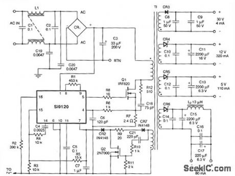
Universal_input_power_supply
Published:2009/7/24 5:19:00 Author:Jessie
This circuit operates directly from 100-, 110-, and 220-V without the use of selector switches or jumpers (permitting the supply to be plugged into wall outlets anywhere in the world). T1 is a Schott Corp. #67122700, L1 is a Renco 1361- 2 common-mode choke, L2 is any 6-μH 1.5-A inductor, and D3 is a 1-A 600-V bridge. (View)
View full Circuit Diagram | Comments | Reading(2510)
Fast_charger_with_linear_regulator_current_source
Published:2009/7/24 5:19:00 Author:Jessie
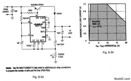
Figure 8-33 shows the MAX713 connected to provide a fast charge (with linear regulation) to both NiCad and NiMH batteries. This circuit solves two closely related problems found in portable power supplies. The circuit charges the battery and switches over from battery power to ac power when an external ac/dc adapter is plugged in. The MAX713 supplies the system load current (while the battery is being charged) by sensing and dynamically regulating the battery current. Figure 8-34 shows the operating area of the circuit. The MAX713 must be programmed for the desired number of cells; charging time, using pin straps, is described in the data sheet. MAXIM BATTERY MANAGEMENT CIRCUIT COLLECTION, 1994, P. 2.
(View)
View full Circuit Diagram | Comments | Reading(1185)
Low_power_bridge
Published:2009/7/24 5:18:00 Author:Jessie
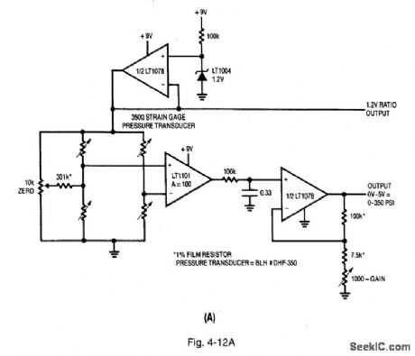
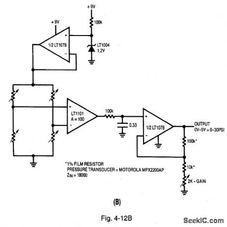
Figure 4-12A is identical to Fig. 4-1, except that the bridge excitation is reduced to 1.2V. This cuts bridge current from about 30 mA to about 3.5 mA. A 0.01% reading of a 10-V powered 350-Ω strain-gauge bridge (Fig. 4-1) requires 3 μV of stable resolution. The Fig. 4-12A circuit requires only 360 nV. Figure 4-12B is similar, but the bridge current is reduced below 700 μA. LINEAR TECHNOLOGY, APPLICATION NOTE 43, P. 18. (View)
View full Circuit Diagram | Comments | Reading(929)
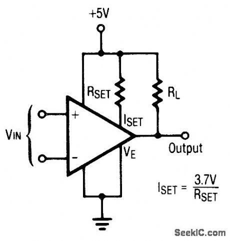
Precision_current_sink_source
Published:2009/7/24 5:16:00 Author:Jessie
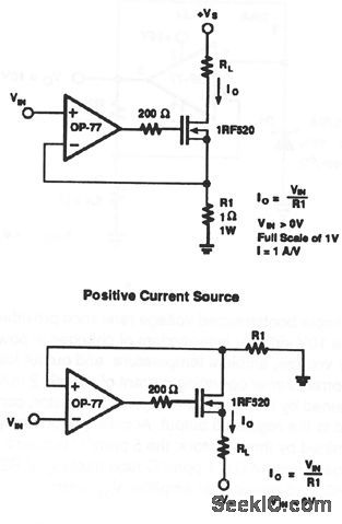
These circuits provide positive current-sink and current-source capability. (View)
View full Circuit Diagram | Comments | Reading(3082)
Extendmg_line_opemted_three_termmal_regulrztor_caypability
Published:2009/7/24 4:39:00 Author:Jessie
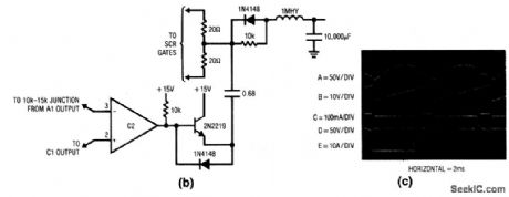
This ac-powered circuit provides 0- to 35-V, 10-A regulation under high-low (90 to 140 Vac) conditions. The transformer output is diode rectified (trace A, Fig. 9-10C), divided down, and used to reset the 0.1-μF capacitor (trace B) via C1. The resulting ramp at C1 is compared to the A1 output by C2. When the ramp exceeds the C2 noninverting input value, C2 goes low and dumps current through the T1 primary (trace C). This fires the appropriate SCR and creates a path from the main transformer to the LC filter (trace D). The resultant current flow (trace E) is limited by the inductor and charges the capacitor. When the ac line cycle drops low enough, the SCR commutates and charging ceases. Figure 9-10B shows a way to trigger the SCRs without a transformer. (View)
View full Circuit Diagram | Comments | Reading(801)
Noninverting_voltage_gain_stage_with_15_V_output
Published:2009/7/24 4:38:00 Author:Jessie
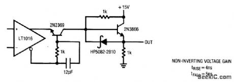
Fig. 15-21 This circuit uses a high-speed comparator (LT1016) and two transistors to provide a fast voltage-gain stage. When the LT1016 switches, the base-emitter voltages at the 2N2369 reverse and cause the transistor to switch rapidly. The 2N3866 emitter follower produces a low-impedance output and the Schottky diode aids current-sink capability, Linear Technology, Linear Applications Handbook 1990, AN13-31. (View)
View full Circuit Diagram | Comments | Reading(718)
Extending_high_voltage_three_terminal_regulator_capability
Published:2009/7/24 4:46:00 Author:Jessie
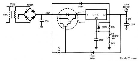
This circuit delivers 100 V at 100 mA and withstands shorts to ground. When an output short occurs, the zener conducts, forcing the Q1 base to 30 V. The Q1 emitter clamps 2 VBE below VZ, well within the VIN/VOUT regulator rating. Q1 sustains 90 VCE at whatever current the transformer and regulator current limit will support. If the regulator and Q1 are thermally coupled, the regulator goes into thermal shutdown and protects the load and regulator as long as the output is shorted. (View)
View full Circuit Diagram | Comments | Reading(787)
Comparator_with_TTL_supply_and_TTL_output
Published:2009/7/24 4:44:00 Author:Jessie
Pig. 15-25 This circuit shows an LP165/365 connected for a TTL supply and a TTL output. Figures 15-24B and 15-24C show the pin connections, and electrical characteristics, respectively. Raytheon Linear Integrated Circuits 1989, p. 5-40. (View)
View full Circuit Diagram | Comments | Reading(713)
Comparator_with_split_supply_and_logic_output
Published:2009/7/24 4:43:00 Author:Jessie

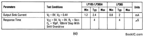
Fig. 15-24 This circuit shows an LP165/365 connected for a split supply, and a logic (TTL) output. Figures 15-24B and 15-24C show the pin connections, and electrical characteristics, respectively. Raytheon Linear Integrated circuits 1989, p. 5-34, 5-36, 5-40. (View)
View full Circuit Diagram | Comments | Reading(692)
Single_supply_fault_monitor
Published:2009/7/24 4:56:00 Author:Jessie
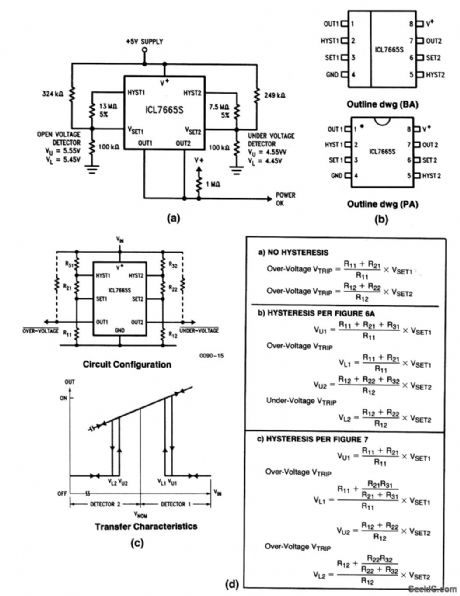
This circuit shows an overvoltage/undervoltage fault monitor for a single supply, using an ICL7665S detector. Figure 9-15B shows the pin connections. The overvoltage trip point is centered around 5.5V, with the undervoltage trip at about 4.5 V. Both points have some hysteresis to prevent erratic output on/off conditions. The two outputs are connected in a wired-Ok signal. Harris Semiconductor, Linear& Telecom ICs, 1991, p 2-131 2137.2138. (View)
View full Circuit Diagram | Comments | Reading(1532)
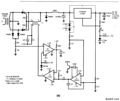
110__to_220_V_regulation_without_switching
Published:2009/7/24 4:52:00 Author:Jessie
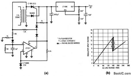
This circuit allows a voltage-regulator to operate on a 110- or 220-V line without having to switch transformer windings. When T1 is driven from 110 V, the LT1011 output goes high and allows the SCR to receive gate bias through the 1.2-kΩ resistor. The 1N4002 is off. T1 output is rectified by the SCR and the regulator sees about 8.5 V at the input. If T1 is plugged into 220 V, the inverting input at the LT1011 is driven beyond 2.5 V, and pin 7 clamps low. This steers the SCR gate bias to ground through the LT1011. The diodes at the LT1011 output prevents reverse voltages from reaching the SCR or the LT1011 output. The SCR goes off and the 1N4002 sources current to the regulator from the T1 center tap. Although the T1 input voltage has doubled, the T1 output is cut in half and regulator power dissipation remains the same. Figure 9-14B shows ac line input versus regulator input-voltage transfer. The switch to center-tap drive occurs midway between 110 and 220 V. (View)
View full Circuit Diagram | Comments | Reading(1153)
Switch_bounce_eliminator_or_filter
Published:2009/7/24 5:28:00 Author:Jessie
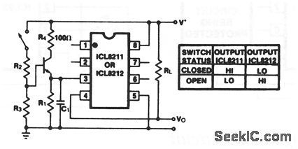
This circuit provides a rapid charge-up of C1 to near V+ on switch closure, and a corresponding slow discharge of C1 on switch break. By proportioning the time constant of R1/C1 to approximately the manufacturer's rated bounce time, the output at terminal 4 of the ICL8211/12 will be a single change of state (no bounce) per switch closure, as shown by the table. (View)
View full Circuit Diagram | Comments | Reading(911)
INVERTING_BIPOLAR_CURRENT_SOURCE_HIGH_SPEED
Published:2009/7/1 2:29:00 Author:May
View full Circuit Diagram | Comments | Reading(699)
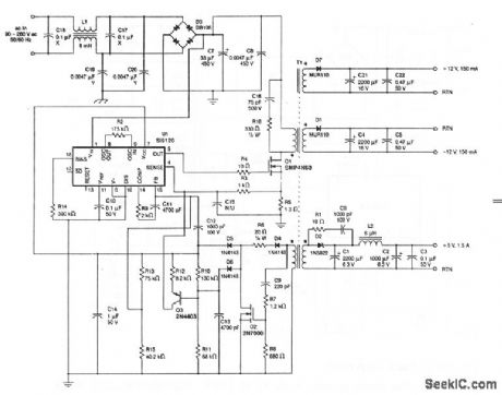
Offline_flyback_converter_
Published:2009/7/24 5:27:00 Author:Jessie
This circuit operates from 90-to 130-V .Regulation is 5% on all output .Ripple is 200 mV p-p on the +30 and +12 outputs ,50 mVp-p on the main +5 output,15 mVp-p on the auxiliay +5 output. power consumptions is 15W.T1 is a Schott Corp.#6712244, L1 is any 8mH common-mode choke, L2 is a Magnetics Inc J40401TC with 6 turn #26 AWG ,and CR1 is any 1-A 600-V bridge. (View)
View full Circuit Diagram | Comments | Reading(2765)
Negative_LCD_contrast_supply
Published:2009/7/24 5:26:00 Author:Jessie
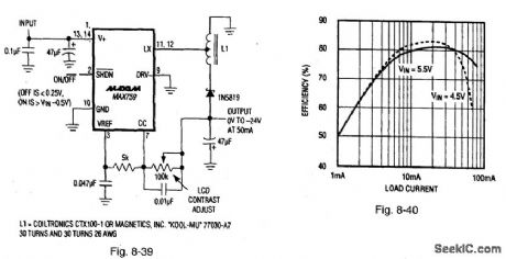
Figure 8-39 shows a MAX759 connected as an LCD-contrast supply with a -24-V output using an autotransformer. Figure 8-40 shows the efficiency curve. The MAX759 has a large lowJsaturation, internal P-channel MOSFET. The use of an autotransformer trades off higher peak switch currents for reduced stress voltage on the switch transistor. The circuit operates over a 4-V to 6-V range (with a maximum input/output differential of 30 V), draws 3.7-mA quiescent current, and is capable of 50-mA output. Mount L1 close to the IC to minimize PC-trace inductance in the LX lead. MAXIM BATTERY MANAGEMENT CIRCUIT COLLECTION, 1994, P. 47, 48.
(View)
View full Circuit Diagram | Comments | Reading(907)
Stand_alone_LCD_contrast_bias_supply_digitally_adjusted
Published:2009/7/24 5:24:00 Author:Jessie
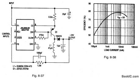
Figure 8-37 shows a MAX749 connected as an LCD-contrast supply with a digitally adjusted negative output. Figure 8-38 shows the efficiency curve. The MAX749 has an on-board five-bit D/A converter that adjusts the LCD contrast voltage (from 1/3 full-scale to full-scale) through a serial interface. No adjustment pots are needed, The circuit operates over a 2-V to 6-V range, draws 310-μA quiescent current, and is capable of 25-mA output. MAXIM BATTERY MANAGEMENT CIRCUIT COLLECTION, 1994, P. 46.
(View)
View full Circuit Diagram | Comments | Reading(781)
Frequency_limit_detector
Published:2009/7/24 5:22:00 Author:Jessie
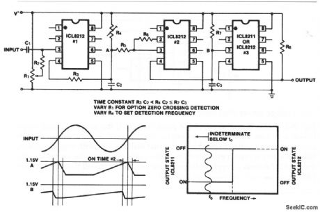
The first ICL8212 is used as a zero-crossing detector. The output circuit (R3, R4, C2) produces a slow positive ramp, where the negative range is much faster than the positive range, as shown. R5 and R6 provide hysteresis so that under all circumstances the second ICL8212 is turned on for sufficient time to discharge C3. The time constant of R7/C3 is much greater than for R4/C2.Depending on the desired output polarities for low and high input frequencies, either an ICL8211 or an ICL8212 can be used as the output driver. (View)
View full Circuit Diagram | Comments | Reading(1405)
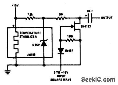
PRECISION_REFERENCE_SQUARE_WAVE_VOLTAGE_REFERENCE
Published:2009/7/1 2:27:00 Author:May
View full Circuit Diagram | Comments | Reading(656)
Sampled_output_bridge_signal_conditioner
Published:2009/7/24 5:21:00 Author:Jessie
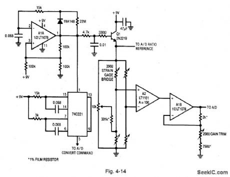
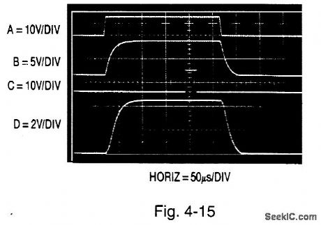
Figure 4-14 shows a bridge signal conditioner with sampled output. (This is an extension of the Fig. 4-13 circuit) Figure 4-15 shows the waveforms. Traces A, B, C, and D show the AIA output, Q1 emitter, 74C221 output, and A2 output, respectively. The strobing action is automated by a clocked sequence. Circuit on time is restricted to 250 μs, at a clock rate of about 2 Hz. This keeps average power consumption down to about 200 μA. Oscillator A1A produces a 250-μs clock pulse every 500 ms (trace A, Fig. 4-15). To calibrate, trim both zero and gain for the appropriate outputs. LINEAR TECHNOLOGY, APPLICATION NOTE 43, P. 20. (View)
View full Circuit Diagram | Comments | Reading(882)
| Pages:154/291 At 20141142143144145146147148149150151152153154155156157158159160Under 20 |
Circuit Categories
power supply circuit
Amplifier Circuit
Basic Circuit
LED and Light Circuit
Sensor Circuit
Signal Processing
Electrical Equipment Circuit
Control Circuit
Remote Control Circuit
A/D-D/A Converter Circuit
Audio Circuit
Measuring and Test Circuit
Communication Circuit
Computer-Related Circuit
555 Circuit
Automotive Circuit
Repairing Circuit