
power supply circuit
Index 156
BILATERAL_CURRENT_SOURCE_1
Published:2009/7/1 2:05:00 Author:May
View full Circuit Diagram | Comments | Reading(613)
PROGRAMMABLE_VOLTAGE_SOURCE_1
Published:2009/7/1 2:02:00 Author:May
View full Circuit Diagram | Comments | Reading(588)
0_V_TO_20_V_POWER_REFERENCE
Published:2009/7/1 2:01:00 Author:May
View full Circuit Diagram | Comments | Reading(553)
Adjustable_dc_dc_step_up_converter15_A
Published:2009/7/25 1:15:00 Author:Jessie

This circuit shows an LAS-6350/6450 used as a step-up converter with an adjustable output. (View)
View full Circuit Diagram | Comments | Reading(731)
1_A_dc_dc_step_down_converter_
Published:2009/7/25 0:27:00 Author:Jessie


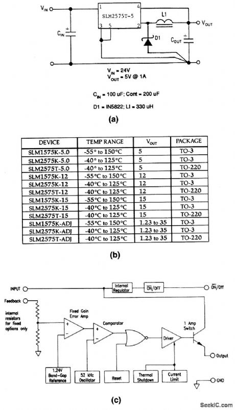
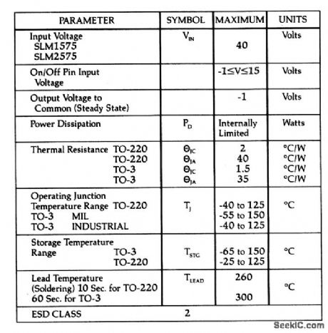
The SLM switching-regulator ICs contain most elements necessary for converter operation, as shown in Fig. 4-2C. Figure 4-2B shows the output voltage and characteristics for various part numbers. Figure 4-2D shows the absolute maximum ratings. Simply add a choke, catch diode, and two capacitors to the IC for a complete converter. (View)
View full Circuit Diagram | Comments | Reading(648)
BILATERAL_CURRENT_SOURCE
Published:2009/7/1 2:00:00 Author:May
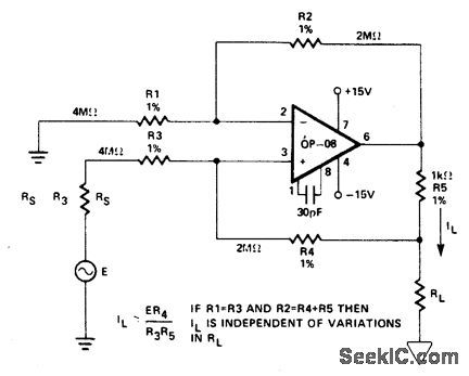
The circuit will produce the current re-lationship to within 2% using 1% values for R1 through R5. This includes variations in RL from 100 ohm to 2000 ohm. The use of large resis-tors for R1 through R4 minimizes the error due to Rt variations. The large resistors are possi-ble because of the excellent input bias current performance of the OP-08. (View)
View full Circuit Diagram | Comments | Reading(0)
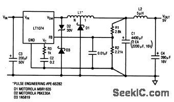
Basic_positive_buck_converter
Published:2009/7/24 8:26:00 Author:Jessie
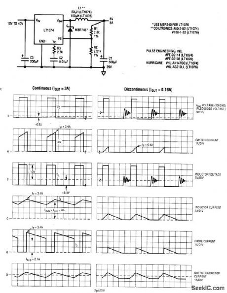
This circuit is used to convert a larger positive input voltage to a lower positive output, using an LT1074 switching regulator. Typical waveforms are shown in Fig. 4-39B. These waveforms are based on a VIN of 20 V, VOUT of 5 V, and L of 50μH for both continuous mode (inductor current never drops to zero) with IOUT of 3A, and discontinuous mode (inductor current drops to zero during a potion of the switching cycle (IOUT =0.17 A). (View)
View full Circuit Diagram | Comments | Reading(787)
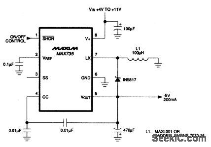
_5_to__5_V_at_220_mA_with_low_power_inverter
Published:2009/7/24 8:58:00 Author:Jessie
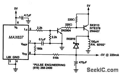
This circuit uses two transistors to buffer the LX output and produce 220-mA of output current. The 2N3904 is used invert the LX output and drive the power pnp. When using external transistor buffers as shown here, the output voltage is set by the external feedback-resistor network ( 180 and 510 kΩ). (View)
View full Circuit Diagram | Comments | Reading(698)
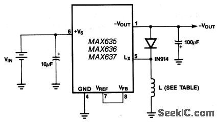
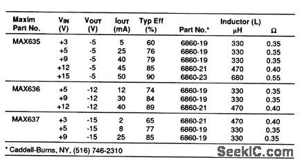
Low_power_inverters
Published:2009/7/24 8:56:00 Author:Jessie
The table of Fig. 4-59B lists measured efficiency and currents of circuits that use the indicated coils and corresponding ICs. (View)
View full Circuit Diagram | Comments | Reading(828)
Low_power_step_down_converters
Published:2009/7/24 8:55:00 Author:Jessie
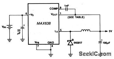
The table of Fig. 4-58B lists measured efficiency and currents of circuits that use the indicated coils. (View)
View full Circuit Diagram | Comments | Reading(633)
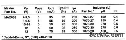
Long_life_IR_drop_voltage_recover_system
Published:2009/7/24 8:53:00 Author:Jessie
This circuit provides a unique solution to a common system-level power-distribution problem. When the supply voltage to a remote board must traverse a long cable, the voltage at the end of the line sometimes drops to unacceptable levels. This circuit solves the problem by taking the reduced voltage at the end of the supply line and boosting it back to +5 V. This can be especially useful in remote-display devices, such as some point-of-sale (POS) terminals, where several meters of cable can separate the terminal from the readout. The 3.2: 1 turns ratio of the transformer allows the MAX631 to provide more than the usual output current, without an external MOSFET, at these relatively low operating voltages. Output current is 150mA at 5 V, with an input of 4 to 5 V. The MAX631 also makes use of the reflected voltage in the transformer primary to generate a higher supply voltage of about +9 V. By operating at 9 V, rather than 5 V, the on resistance of LX is reduced. (View)
View full Circuit Diagram | Comments | Reading(643)
Simple_boost_regulator
Published:2009/7/24 8:34:00 Author:Jessie
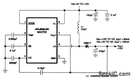
In this circuit,a MAX733 provides a+15-V output at 90 mA inputs from+4.5 to+12 V)or at 120 mA(for inputs from+6 to+12 V). (View)
View full Circuit Diagram | Comments | Reading(681)
Simple_buck_regulator_with_two_outputs
Published:2009/7/24 8:33:00 Author:Jessie

In this circuit, a MAX738 provides a +5-V 200-mA output through the inductor primary, and a + 12-V 30-mA output through the inductor secondary for inputs from 8 to 15 V . (View)
View full Circuit Diagram | Comments | Reading(895)
Simple_buck_regulator
Published:2009/7/24 8:31:00 Author:Jessie
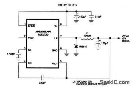
In this circuit, a MAX730 provides a 5-V, 300-mA output for inputs from 6 to 10V . (View)
View full Circuit Diagram | Comments | Reading(626)
Simple_inverter_with_negative_output
Published:2009/7/24 8:30:00 Author:Jessie
In this circuit, a MAX739 current-mode PWM regulator provides all of the active circuitry needed to invert a positive input (+4 to +10 V) to a negative output (-5 V at 200 mA), with a minimum of external components. A switching frequency of 165-kHz allows for small external components. (View)
View full Circuit Diagram | Comments | Reading(772)
Tapped_inductor_buck_converter
Published:2009/7/24 8:28:00 Author:Jessie
This circuit uses a tapped inductor to increase the current output capability. The ratio of input turns to output turns is N. With an N of 3 (three times as many turns to the left of D 1 as at the right of D 1 ), a VIN of 20 V, an L of 100μH, and a VOUT of 5 V, the IOUT is approximately 10 A (double that of Fig. 4-39). (View)
View full Circuit Diagram | Comments | Reading(1074)
Dc_dc_converter_1
Published:2009/7/24 5:33:00 Author:Jessie
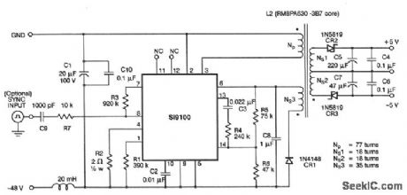
This circuit is similar to that of Fig. 4-22, except that a 3-W Si9100 is used instead of a 1-W Si9105 as the switchmode regulator. Notice that the sync input (at pins 7 and 8) is optional for both circuits. (View)
View full Circuit Diagram | Comments | Reading(705)
LCD-contrast_supply_for_color_displays
Published:2009/7/24 5:32:00 Author:Jessie
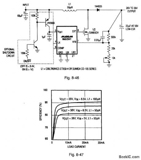
Figure 8-46 shows a MAX641 connected as an LCD-contrast supply with positive26-V to 38-V output (primarily for color displays). Figure 8-47 shows the efficiencycurves.The circuit operates over a 4.5-V to 15-V(five-to eight-cell)range, draws550 μA (with 5-V in and 26-V output) or 1-mA (with 9.6-V input and 38-V output) quiescent current and is capable of 30-mA output,Load regulation is 0.16%/mA, line regulation is 0.16%/V output. and output noise is 200 mV p-p.The input range makesthe circuit suitable for+5 -V regulated input or for a direct-battery connection. For input voltages above 7 V substitute a 100-μH inductor (Coiltronix CTS100-4) to maintain low output nolse and ripple.MAXIM BATTERY MANAGEMENT CIRCUITCOLLECTION. 1994 P.50. (View)
View full Circuit Diagram | Comments | Reading(667)
Time_domain_bridge
Published:2009/7/24 5:31:00 Author:Jessie
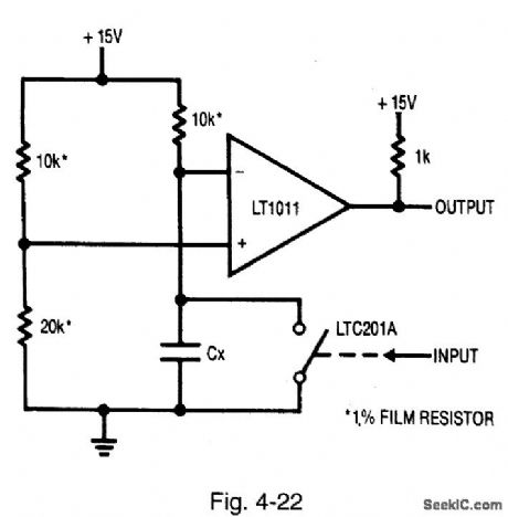

Figure 4-22 shows a bridge circuit that operates in the time domain, and is particularly suitable for capacitance measurement. With S1 closed, the comparator output is high. When S1 opens, capacitance Cx charges. When the Cx potential crosses the voltage established at the comparator noninverting input, the comparator output goes low. The elapsed time between the switch opening and the comparator going low is proportionate to the Cx, value. The circuit is insensitive to supply and repetition rate variations, and can provide good accuracy if the time constants are kept much larger than comparator and switch delays. The LT1011 delay is about 200 ns, and the LTC201A delay is about 450 ns. To ensure 1% accuracy, the time constant of Cx and the series resistor should not go below 65 μs.Extremely low values of capacitance might be influenced by switch charge injection.In such cases, switching should be implemented by alternating the bridge drive between ground and +15 V. LINEAR TECHNOLOGY, APPLICAION NOTE 43, P. 27. (View)
View full Circuit Diagram | Comments | Reading(873)
Dc_dc_forward_converter
Published:2009/7/24 5:30:00 Author:Jessie
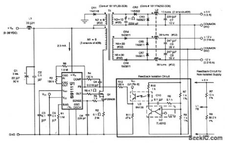
The feedback isolation circuit (shown within the box) can be replaced by the simple R7/R8 voltage feedback divider if the supply-output feedback does not need to be isolated from the load. (View)
View full Circuit Diagram | Comments | Reading(801)
| Pages:156/291 At 20141142143144145146147148149150151152153154155156157158159160Under 20 |
Circuit Categories
power supply circuit
Amplifier Circuit
Basic Circuit
LED and Light Circuit
Sensor Circuit
Signal Processing
Electrical Equipment Circuit
Control Circuit
Remote Control Circuit
A/D-D/A Converter Circuit
Audio Circuit
Measuring and Test Circuit
Communication Circuit
Computer-Related Circuit
555 Circuit
Automotive Circuit
Repairing Circuit