
power supply circuit
Index 148
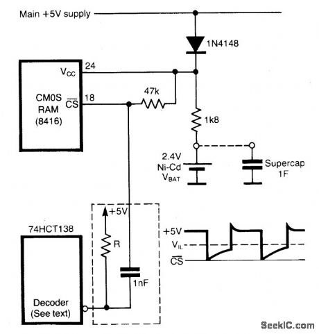
STAND_BY_POWER_FOR_NON_VOLATILE_CMOS_RAMs
Published:2009/7/2 4:46:00 Author:May
Circuit Notes
To prevent loss of data when a CMOS RAM is switched from normal operation (VCC=5 volts) to stand-by mode (VCC=VgAT) it must be ensured that the CS pin goes near the VCC rail at all times. Ac coupling to the chip select is made through capacitor C, breaking the dc current path between Vgg (and hence VgAT) and the decoder output. So, whatever the impedance state of the decoder in power down, the battery will provide current only for the RAM, low enough to keep the voltage at CS near to VCC. (View)
View full Circuit Diagram | Comments | Reading(786)
Micropower_post_regulated_switching_regulator
Published:2009/7/24 2:21:00 Author:Jessie
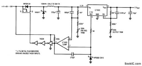
This circuit operates for a 6- or 9-V battery and provides 5-V output at 50 mA (even though the quiescent current is 40 μA). (View)
View full Circuit Diagram | Comments | Reading(798)
LOW_LEVEL_RF_SOURCE
Published:2009/7/2 4:39:00 Author:May
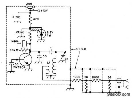
Used to measure noise floor of receiver under test. RF source is simple, well-shielded crystal-controlled oscillator that is decoupled from battery supply. After attenuator resistors are adjusted to provide about S7 signal in receiver, oscillator housing is sealed with solder. Once calibrated, RF source is comparable to commercial signal generator, as leakage is quite low. Output is.-112 dBm at 14 MHz. L1 has 24 turns enamel on Amidon T5O-6 toroid. with 1 turn for output link.-W. Hayward. Defining and Measuring Receiver Dynamic Range. QST. July 1975. p 15-21 and 43. (View)
View full Circuit Diagram | Comments | Reading(1011)
12_V_buck_boost_from_a_45_V_to_15_V_input
Published:2009/7/24 2:25:00 Author:Jessie
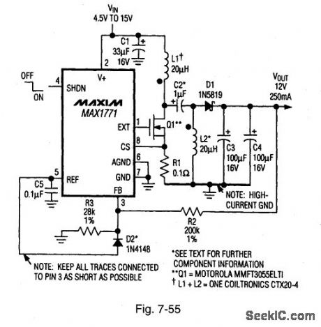
Figure 7-55 shows the MAX1771 connected to provide a 12-V output at 250 mA, with a 4.5-V to 15-V input. See Fig. 7-51 for component suppliers. MAXIM NEW RELEASES DATA Book, 1995, P. 4-26. (View)
View full Circuit Diagram | Comments | Reading(1396)
Step_up_down_for_5_V_33_V_output
Published:2009/7/24 2:22:00 Author:Jessie
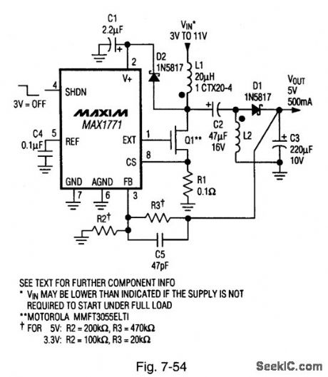
Figure 7-54 shows the MAX1771 connected to provide either 5-V or 3.3-V output at 0.5 A, with a 3-V to 11-V input. See Fig. 7-51 for component suppliers. MAXIM NEW RELEASES DATA Book, 1995, P. 4-25. (View)
View full Circuit Diagram | Comments | Reading(809)
POWER_SUPPLY_FOR_25_WATT_ARC_LAMP
Published:2009/7/2 4:01:00 Author:May
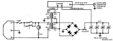
Circuit NotesA dual-voltage circuitry both strikes and maintains the arc.The lamps require a starting voltage in excess of 1,000 volts. Once stabilized, the voltage drop across the lamp is near 20 volts. Power supply consists of two main sections. The first section, the low-voltage power supply section, is an 84-volt direct-current supply.This supply powers the stabilized arc. Current is limited by the 10 ohm adjustable and 25 ohm fixed resis-tance. The second section, the high-voltage starter circuit, is a Cockroft-Walton voltage multiplier. With no load, the output voltage is 2,036 volts. However, when the arc is established, the heavy current drain maintains a forward bias on all of the diodes, and the circuit becomes a straight path with a voltage drop of 7.2 volts. The small value of the capacitors used in the multiplier guarantees that the diodes will be forward-biased once the arc is established. (View)
View full Circuit Diagram | Comments | Reading(1574)
High_efficiency_inverter_with_adjustable_output
Published:2009/7/24 2:48:00 Author:Jessie
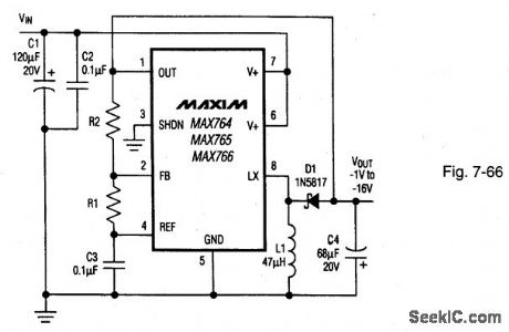
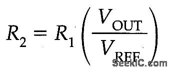
Figure 7-66 shows the MAX764/65/66 connected to provide inverter operation with an adjustable output (-1.0 V to -16 V). For adjustable operation, let R1= 150 kΩ, then find the value of R2 using: Where VREF = 1.5 V. See Fig. 7-65 for component suppliers. MAXIM NEW RELEASES DATA Book, 1995, P. 4-121. (View)
View full Circuit Diagram | Comments | Reading(959)
BIPOLAR_POWER_SUPPLY_FOR_BATTERY_INSTRUMENTS
Published:2009/7/2 3:54:00 Author:May
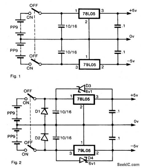
Circuit NotesTo generate regulated ±5-V supplies from a pair of dry batteries, the circuit of Fig.1 is commonly used. In order to give protection from inadvertent reverse connection of a battery, a diode in series with each battery would produce an unacceptable voltage drop. The more effective approach is to fit diodes D1 and D2 as shown in Fig. 2, in parallel with each battery.When the supply is switched off, there is the risk of a reverse bias being applied across the regulators, if there is significant inductance or capacitance in the load circuit.Diodes across the regulators prevent damage. When the power supply is switched on, the two switches do not act in unison. There is a probability that one or the other regulators will be latched hard off by the other. To prevent this, D3 and D4 are Zener diodes so that ±5-V rails are pulled up by the batteries until the regulators establish the correct levels. (View)
View full Circuit Diagram | Comments | Reading(1077)
400_VOLT,60_WATT_PUSH_PULL_POWER_SUPPLY_
Published:2009/7/2 3:43:00 Author:May
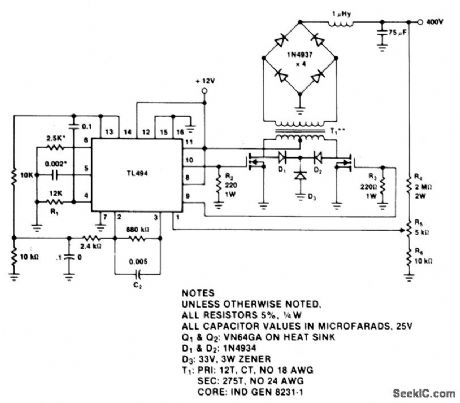
Circuit Notes
The design delivers a regulated 400-V, 60-W output. The TL494 switching regulator governs the opdrating frequency and regulates output voltage. R1 and C1 determine switching frequency, which is approximately 0.5RC-100 kHz for the values shown. The TL494 directly drives the FET's gates with a voltage-controlled, pulse-width-modulated signal. After fullwave rectification, the output waveform is filtered by a chokeinput arrangement. The 1 μH, 75 μF filter accomplishes the job nicely at 100 kHz. A feedback scheme using R4, R5 and R6 provides for outputvoltage regulation adjustment, with loop compensation handled by C2. Diodes D1 and D2 provide isolation and steering for the 33-V zener transient clamp, D3. Output regulation is typically 1.250/0 from noload to the full 60-W design rating. Regulation is essentially determined by the TL494. Output noise and ripple consists mainly of positive and negative 0.8-V spikes occurring when the output stage switches. (View)
View full Circuit Diagram | Comments | Reading(6991)
BENCH_TOP_POWER_SUPPLY
Published:2009/7/2 3:38:00 Author:May
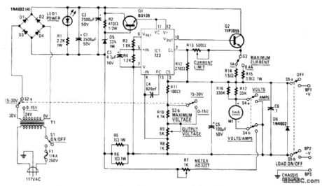
Circuit Notes
A tapped transformer drives a diode bridge (D1-D4) and two 2500 pF filter capacitors (C1 and C2), that provide a noload voltage of 37 or 47 volts, depending upon the position of switch 52a. The unregulated dc is then fed to a pre-regulator stage composed of Q1 and D5. Those components protect IC1(the 723)from an over-voltage condition; the 723 can't handle more than 40 volts. The LED (LEDl) and its 2.2 k current-limiting resistor(R1)provide on/off indication. The current through the LED varies slightly according to the transformer tap selected, but that's of no real consequence. The series-pass transistor in IC1 drives voltage-follower Q2, providing current amplification. The transistor can handle lots of power. It has a maximum collector current of 15 amps and a maximum VCE of 70V, both of which are more than adequate for our supply. (View)
View full Circuit Diagram | Comments | Reading(2468)
BASIC_SINGLE_SUPPLY_VOLTAGE_REGULATOR
Published:2009/7/2 3:26:00 Author:May
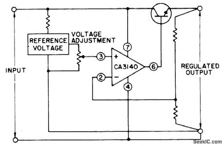
Circuit NotesThe circuit uses a CA3140 BiMOS op amp capable of supplying a regulated output that can be adjusted from essentially 0 to 24 volts. (View)
View full Circuit Diagram | Comments | Reading(788)
MICROPOWER_BANDGAP_REFERENCE_SUPPLY
Published:2009/7/2 3:16:00 Author:May
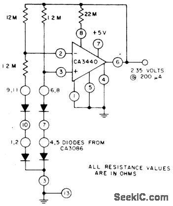
Circuit NotesThe circuit uses a CA3440 BiMOS op amp and CA3086 transistor array. The no-load current from 5-volt supply is 1.5 μA. Load current can go as high as 200 pA and still maintain output voltage regulation within 0.05%. (View)
View full Circuit Diagram | Comments | Reading(697)
Battery_status_indicator
Published:2009/7/24 2:32:00 Author:Jessie
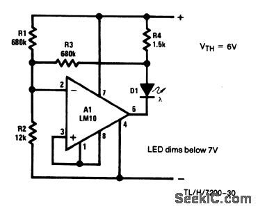
This circuit is designed for a 9-V battery. D1 begins dimming noticeably below 7 V and extinguishes at 6 V. If the dimming function is not required, remove R3 and make R1 340 kΩ. D1 will then remain at normal brilliance until the battery goes below 6 V. (View)
View full Circuit Diagram | Comments | Reading(0)
SWITCH_MODE_POWER_SUPPLY
Published:2009/7/2 3:15:00 Author:May
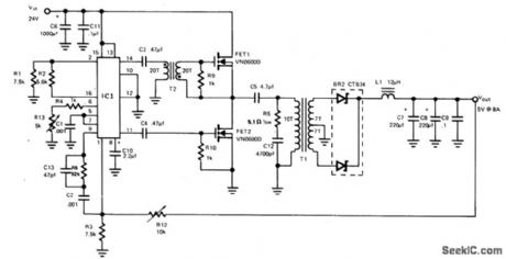
Circuit NotesThis buck-derived circuit provides up to 8 A at 5 Vdc operating off 24 to 32 Vdc.The two power MOSFETs in the circuit conduct alternately for equal periods. Switching frequency is 150 kHz, set by the PWM125 controller. Output of the two MOSFETs is transformed to a lowvoltage level, then rectified. Efficiency of the circuit is 75% when operated in a 22 to 32 V range. Efficiency approaches 90% with higher voltage inputs. (View)
View full Circuit Diagram | Comments | Reading(1775)
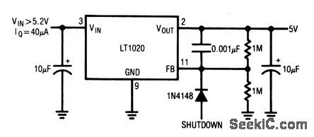
Battery_backup_regulator
Published:2009/7/24 2:32:00 Author:Jessie
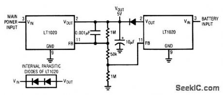
This circuit shows a low-loss way to implement a glitch-free battery backup for a memory or similar circuit. The feedback string is arranged so that one LT1020 does not conduct under line-powered conditions. When the line goes down, the line LT1020 begins to go off, which allows the battery-driven LT1020 to turn on and maintain the load. (View)
View full Circuit Diagram | Comments | Reading(676)
RADIATION_HARDENED,125_A_LINEAR_REGULATOR
Published:2009/7/2 3:10:00 Author:May
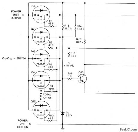
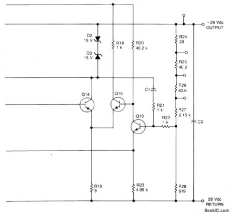

Circuit NotesIntended for extreme temperature, radiation-hardened environments, this linear supply is capable of supplying 28 Vdc at 125 A from an acdriven power unit.In operation, power supply output voltage is sensed by the voltage divider consisting of R24 to R28 and fed to one input of a discrete differential amplifier composed of Q13 through Q16. The other input of the amplifier is connected to a radiation-hardened zener diode, D1. Local feedback using R21 and C1 produces gain to phase shift that are independent of individual component parameters, which provides stable operation into the required loads. (View)
View full Circuit Diagram | Comments | Reading(710)
CMOS_monolithic_voltage_converter
Published:2009/7/24 2:30:00 Author:Jessie
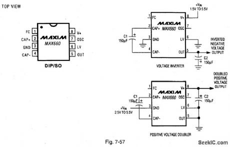
Figure 7-57 shows a MAX660 connected to provide either voltage inversion or positive voltage doubling. The conversion efficiency is a typical 88% at 100 mA, with a typical loss of 0.65 V. The typical output impedance is 6.5Ω. The operating current is 120 μA. MAXIM NEW RELEASES DATA Book, 1995, P. 4-73.
(View)
View full Circuit Diagram | Comments | Reading(712)
Micropower_regulator_shutdown
Published:2009/7/24 2:29:00 Author:Jessie
This circuit shows a simple way to shut an LT1020 regulator down. In this state, the regulator draws only 40 μA. (View)
View full Circuit Diagram | Comments | Reading(643)
_12_1__and__20_V_dual_supply
Published:2009/7/24 2:41:00 Author:Jessie
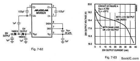
Figure 7-62 shows the MAX662A flash-memory supply (Figs. 7-58 through 7-61) used as a dual power supply. Figure 7-63 shows the output-current characteristics. Maxnvt NEW RELEASES DATA Book, 1995, P.4-80. (View)
View full Circuit Diagram | Comments | Reading(557)
EXCESS_NOISE_SOURCE
Published:2009/7/2 2:21:00 Author:May
Develops about 18 dB of excess noise in region of 50-300 MHz for optimizing converter or receiver for best noise figure. Can also be used for noise optimizing of TV receivers and for peaking UHF TVfront ends. Q1 and Q2 form cross-coupled 7OO-CR1 MVBR. C1 is greater than C2 to favor conduction of Q2. When Q2 is on, Q3 turns on and makes current flow through broadband noisediode CR1. Diode is forward-biased because available gating voltage does not generate enough noise in reversebias mode. If noise output is too great, insert 20000-ohm attenuator as shown.-T. E. Hartson, A Gated Noise Source, QST, Jan. 1977. p 22-23. (View)
View full Circuit Diagram | Comments | Reading(888)
| Pages:148/291 At 20141142143144145146147148149150151152153154155156157158159160Under 20 |
Circuit Categories
power supply circuit
Amplifier Circuit
Basic Circuit
LED and Light Circuit
Sensor Circuit
Signal Processing
Electrical Equipment Circuit
Control Circuit
Remote Control Circuit
A/D-D/A Converter Circuit
Audio Circuit
Measuring and Test Circuit
Communication Circuit
Computer-Related Circuit
555 Circuit
Automotive Circuit
Repairing Circuit