
Signal Processing
Index 29
TV transmitter circuit
Published:2012/11/15 20:49:00 Author:muriel | Keyword: TV , transmitter circuit
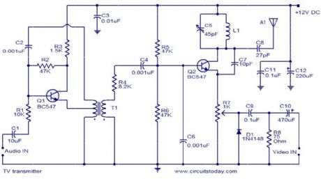
The TV transmitter given here uses UK standard 1 FM modulation for sound and PAL for video modulation. The audio signal to be modulated is pre-amplified using the transistor Q1 and associated components. The transistor Q2 has two jobs: production of carrier frequency and modulation. The pre-amplified audio signal is fed to the base of transistor Q2 for modulation. Capacitor C5 and inductor L1 forms the tank circuit which is responsible for producing the carrier frequency. The video signal is fed to the emitter of transistor Q2 via POT R7 for modulation. The modulated composite signal (audio+video) is transmitted by the antenna A1.
Notes: Assemble the circuit on a good quality PCB. Inductor L1 can be made by making 4 turns of 24SWG enameled copper wire on a 6mm dia: plastic former. T1 can be a radio frequency transformer with built in capacitor. (Can be found on old transistor radio boards). Antenna A1 can be a 1M long copper wire. (Experiment with the length to get optimum performance). This transmitter is working in VHF band somewhat between 50 � 210MHz. This transmitter is compatible only with PAL B and PAL G systems. (View)
View full Circuit Diagram | Comments | Reading(1915)
TV Transmitter2
Published:2012/11/15 20:48:00 Author:muriel | Keyword: TV, Transmitter
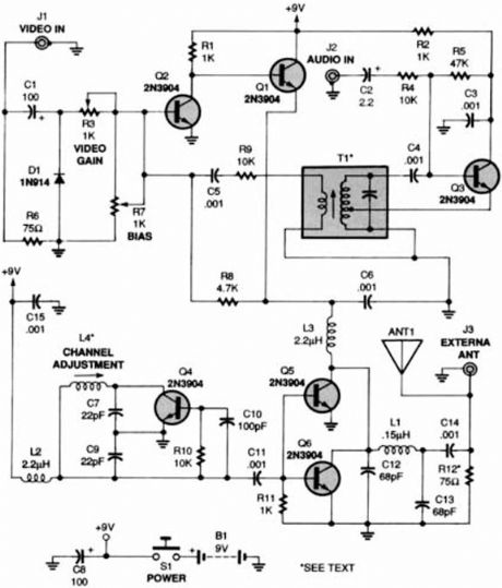
One of the most useful gadgets a video enthusiast can have is a low-power TV Transmitter. Such a device can transmit a signal from a VCR to any TV in a home or backyard. Imagine the convenience of being able to sit by the pool watching your favorite movie on a portable with a tape or laser disc playing indoors. You could even retransmit cable TV for your own private viewing. (View)
View full Circuit Diagram | Comments | Reading(1111)
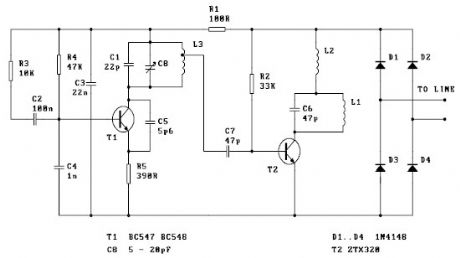
TV Transmitter
Published:2012/11/15 20:48:00 Author:muriel | Keyword: TV, Transmitter
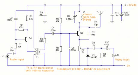
A VHF band TV transmitter using negative sound modulation and PAL video modulation. This is suitable for countries using TV systems B and G. (View)
View full Circuit Diagram | Comments | Reading(1815)
TV Audio Video Transmitter
Published:2012/11/15 20:47:00 Author:muriel | Keyword: TV , Audio , Video, Transmitter
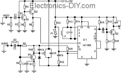
This TV transmitter transmits audio and video signal from Camcoder Camera, DVD, VHS, Satellite, video game, etc. Playing them in a channel free from the strip of VHF. These signal can be radiated with a common antenna and captured in an it distances of until about 500 meters that it is the most appropriate for urban areas, reminding that and necessary to be a lot of caution and careful for not interfering in frequencies of other issuing, as well as to emergency services. Depending on the local conditions (existence or not of obstacles). Fed with tensions from 12 to 15 Volts, the circuit has excellent I carry out so much in the emission of monochrome signal, as in colors. An important point of this project 倀he easiness with that he can be set up and adjusted, since only two coils are used. Ideal to be used with surveillance cameras turning the without thread. As it Works the tv video and audio transmitter with lm1889n The heart of this circuit transmitter 俰s the integrated circuit LM1889N of National Semiconductor, that consists of a Modulator of Video for TV in an involucres of 18 pins DIL. (View)
View full Circuit Diagram | Comments | Reading(2142)
Telephone FM Transmitter
Published:2012/11/15 20:46:00 Author:muriel | Keyword: Telephone, FM , Transmitter
This FM transmitter attaches in series to one of your phone lines. When there is a signal on the line (that is, when you pick up the handset) the circuit will transmit the conversation. In particular it will radiate from the phone line itself. It is a passive device - there is no battery. It uses the signal on the phone line for power. No aerial is needed - it feeds back the RF signal into the phone line which radiates it in the FM band. The frequency of transmission may be adjusted by the trimcap. (View)
View full Circuit Diagram | Comments | Reading(1032)
Stereo FM Transmitter circuit with BA1404
Published:2012/11/15 20:45:00 Author:muriel | Keyword: Stereo , FM , Transmitter , BA1404
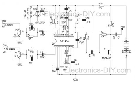
With this Stereo FM Transmitter with BA1404 you will be able to create a mini stereo FM station and broadcast to your entire home, a simple way to have an audio link wireless with ease. With the FM transmitter BA1404 Hifi Stereo you can stream your music from your iPod MP3, satellite receiver, computer, DVD player, Mobile Phone, MP4 player and MP3 and other audio source directly to an FM receiver with crystal clear sound. (View)
View full Circuit Diagram | Comments | Reading(5819)
Stereo FM Transmitters with BA1404
Published:2012/11/15 20:43:00 Author:muriel | Keyword: Stereo , FM, Transmitters, BA1404
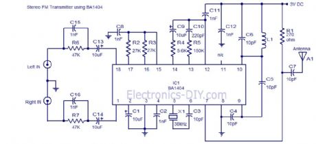
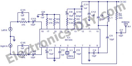
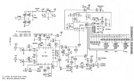
A high quality stereo FM transmitter circuit is shown here. The circuit is based on the IC BA1404 from ROHM Semiconductors. BA1404 is a monolithic FM stereo modulator that has built in stereo modulator, FM modulator and RF amplifier. The FM modulator can be operated from 76 to 108MHz and power supply for the circuit can be anything between 1.25 to 3 volts. In the circuit R7, C16, C14 and R6, C15, C13 forms the pre-emphasis network for the right and left channels respectively. This is done for matching the frequency response of the FM transmitter with the FM receiver. Inductor L1 and capacitor C5 is used to set the oscillator frequency. Network C9,C10, R4,R5 improves the channel separation. 38kHz crystal X1 is connected between pins 5 and 6 of the IC. Composite stereo signal is created by the stereo modulator circuit using the 38kHz quartz controlled frequency.
Assemble the circuit on a good quality PCB. Powering the circuit from a battery will reduce noise. Use an 80 cm copper wire as antenna. For L1 make 3.5 turns of 0.5mm dia enamelled copper wire on a 5mm dia ferrite core.
(View)
View full Circuit Diagram | Comments | Reading(1181)
Stereo FM Transmitter with BA1404
Published:2012/11/15 20:42:00 Author:muriel | Keyword: Stereo , FM, Transmitter , BA1404
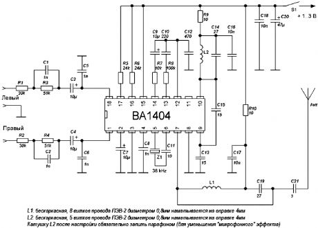
Circuit of stereo FM transmitter of of high quality using integrated circuit ba1404 for mp3, mp4, ipod, computer, radio of the car. Transmit of your equipment of portable audio for the radio of your car, transmitters of fm of low potency are the ideal for transmission wireless of audio sign for fm receivers. Mainly in that case that is treated of transmitter of FM stereo with ba1404. The heart of that circuit is the circuit integrated ba1404, that is a mini fm transmitter, that already counts with the necessary internal circuits for transmission in fm. just being necessary to increase some components discman or any other audio source turning the wireless. If you already set up other transmitters of transistorized fm it will see that when setting up that with having integrated BA1404, that the quality of the sound and the frequency stability is excellent. Besides the but it presents easy assembly. (View)
View full Circuit Diagram | Comments | Reading(2950)
Stereo FM Transmitter Using BA1404
Published:2012/11/15 20:40:00 Author:muriel | Keyword: Stereo , FM , Transmitter, BA1404
A high quality stereo FM transmitter circuit is shown here. The circuit is based on the IC BA1404 from ROHM Semiconductors. BA1404 is a monolithic FM stereo modulator that has built in stereo modulator, FM modulator, RF amplifier circuitry. BA1404 FM transmitter can be operated from 76 to 108MHz and power supply for the circuit can be anything between 1.25 to 3 volts.
In the circuit R7, C16, C14 and R6, C15, C13 forms the pre-emphasis network for the right and left channels respectively. This is done for matching the frequency response of the FM transmitter with the FM receiver. Inductor L1 and capacitor C5 is used to set the oscillator frequency. Network C9,C10, R4,R5 improves the channel separation. 38kHz crystal X1 is connected between pins 5 and 6 of the IC. Composite stereo signal is created by the stereo modulator circuit using the 38kHz quartz controlled frequency. (View)
View full Circuit Diagram | Comments | Reading(2434)
Spy FM Transmitter Bug
Published:2012/11/15 20:40:00 Author:muriel | Keyword: Spy , FM , Transmitter Bug

Here's a tiny one transistor spy FM transmitter bug that operates from a single 1.5V AA battery. Main advantage of this circuit is that power supply is a 1.5 Volts cell (any size) which makes it possible to fix PCB and the battery into very tight places. Transmitter even runs with standard NiCd rechargeable cells, for example a 750mAh AA size battery runs it about 500 hours (while it draws 1.4mA at 1.24V) which equals to 20 days. This way circuit especially valuable in amateur spy operations. Mini FM transmitters take place as one of the standard circuit types in an amateur electronics fan's beginning steps. When done right, they provide very clear wireless sound transmission through an ordinary FM radio over a remarkable distance. I've seen lots of designs through the years, some of them were so simple, some of them were powerful, some of them were hard to build etc. (View)
View full Circuit Diagram | Comments | Reading(1445)
Simple FM Transmitter Bug
Published:2012/11/15 1:01:00 Author:muriel | Keyword: Simple , FM , Transmitter Bug
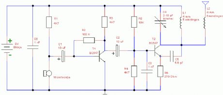
This is a simple design of a small FM Transmitter Bug that's perfect for transmitting and eavesdropping purposes. Due to the high sensitivity, even the ticking of the clock to hear. The range is estimated at anything from 50 meters. With a small piece of wire as an antenna to get at least the whole house. L1 and L2 are two equal air pools. They each consist of 5 turns at a diameter of about 4 mm. The thickness of the wire does not matter, 0.5 mm works perfectly. C4 is the frequency adjustment. Tune an FM radio in an empty area of the FM band and C4 to turn your silence or hear a whistle. From what you can precisely adjust the radio and the transmitter installed in a room somewhere to intercept. Note: Because these transmitter bugs inherently unstable, you better read the short legs of the components keep the circuit mechanically tightly together up. Also placing a 1 nF capacitor (C6) will benefit stability. R1, R3, R4: 4K7 R2: 100K R5: 10K R6: 270 Ohms C1, C2: 10 uF C3, C6: 1 nF C4: 2-18 pF trimmer C5: 5.6 pF L1, L2: air puddle windings on May 4 mm in diameter (see text) T1, T2: 547 BC Condenser microphone Original Text: Ook het plaatsen van een 1 nF condensatortje (C6) over de voedingsaanluitingen komt de werking ten goede. (View)
View full Circuit Diagram | Comments | Reading(2111)
Simple FM Transmitter circuit
Published:2012/11/15 1:00:00 Author:muriel | Keyword: Simple , FM, Transmitter circuit
Mini FM transmitters take place as one of the standard circuit types in an amateur electronics fan's beginning steps. When done right, they provide very clear wireless sound transmission through an ordinary FM radio over a remarkable distance. I've seen lots of designs through the years, some of them were so simple, some of them were powerful, some of them were hard to build etc. Here is the last step of this evolution, the most stable, smallest, problem-less, and energy saving champion of this race. Circuit given below will serve as a durable and versatile FM transmitter till you break or crush it's PCB. Frequency is determined by a parallel L-C resonance circuit and shifts very slow as battery drains out. (View)
View full Circuit Diagram | Comments | Reading(1232)
Simple FM Transmitter
Published:2012/11/15 0:58:00 Author:muriel | Keyword: Simple , FM , Transmitter

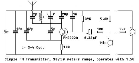
Simple FM transmitter with a single transistor. Mini FM transmitters take place as one of the standard circuit types in an amateur electronics fan's beginning steps. When done right, they provide very clear wireless sound transmission through an ordinary FM radio over a remarkable distance. I've seen lots of designs through the years, some of them were so simple, some of them were powerful, some of them were hard to build etc.
Here is the last step of this evolution, the most stable, smallest, problemless, and energy saving champion of this race. circuit given below will serve as a durable and versatile FM transmitter till you break or crush it's PCB. Frequency is determined by a parallel L-C resonance circuit and shifts very slow as battery drains out. Schematic Simple FM Transmitter involves on a single transistor oscillator Technical datas: Supply voltage : 1.1 - 3 Volts Power consumption : 1.8 mA at 1.5 Volts Range : 30 meters max. at 1.5 Volts Main advantage of this circuit is that power supply is a 1.5Volts cell (any size) which makes it possible to fix PCB and the battery into very tight places. Transmitter even runs with standard NiCd rechargeable cells, for example a 750mAh AA size battery runs it about 500 hours (while it drags 1.4mA at 1.24V) which equals to 20 days. This way circuit especially valuable in amateur spy operations :) Transistor is not a critical part of the circuit, but selecting a high frequency / low noise one contributes the sound quality and range of the transmitter. PN2222A, 2N2222A, BFxxx series, BC109B, C, and even well known BC238 runs perfect. Key to a well functioning, low consumption circuit is to use a high hFE / low Ceb (internal junction capacity) transistor. Not all of the condenser microphones are the same in electrical characteristics, so after operating the circuit, use a 10K variable resistance instead of the 5.6K, which supplies current to the internal amplifier of microphone, and adjust it to an optimum point where sound is best in amplitude and quality. Then note the value of the variable resistor and replace it with a fixed one. The critical part is the inductance L which should be handmade. Get an enameled copper wire of 0.5mm (AWG24) and round two loose loops having a diameter of 4-5mm. Wire size may vary as well. Rest of the work is much dependent on your level of knowledge and experience on inductances: Have an FM radio near the circuit and set frequency where is no reception. Apply power to the circuit and put a iron rod into the inductance loops to chance it's value. When you find the right point, adjust inductance's looseness and, if required, number of turns. Once it's OK, you may use trimmer capacitor to make further frequency adjustments. You may get help of a experienced person on this point. Do not forget to fix inductance by pouring some glue onto it against external forces. If the reception on the radio lost in a few meters range, than it's probably caused by a wrong coil adjustment and you are in fact listening to a harmonic of the transmitter instead of the center frequency. Place radio far away from the circuit and re-adjust. An oscilloscope would make it easier, if you know how to use it in this case. Unfortunately I don't have any :( Every part should fit on the following PCB easily. Pay attention to the transistor's leads which should be connected right. Also try to connect trimmer capacitor's moving part to the + side, which may help unwanted frequency shift while adjusting. PCB drawing should be printed at 300DPI, here is a TIFF file already set. The one below is a past PCB work of mine, which was prepared to fit into a pocket flashlight. Since it was so crowded, use the new computerized PCB artwork instead, yet very small. Take a look at my PCB design page to get information on my work style. Here is a completed and perfectly running circuit, mounted in a pocket light, taking the advantage of the 1.5V AA cell slot near it. Microphone is fixed into the bulb's place and antenna is made out of a 30cm soft cable. When cover is placed, it becomes very handy! Do not forget, restrictions on radio frequency transmitting devices may differ in your local area. This circuit has a power output that should be less than 1mW so have to be safe under many kinds of legal conditions but particular attempts such as listening to other people's private life will always be disapproved everywhere. (View)
View full Circuit Diagram | Comments | Reading(4511)
Sensitive FM Transmitter Bug
Published:2012/11/15 0:58:00 Author:muriel | Keyword: Sensitive, FM , Transmitter Bug
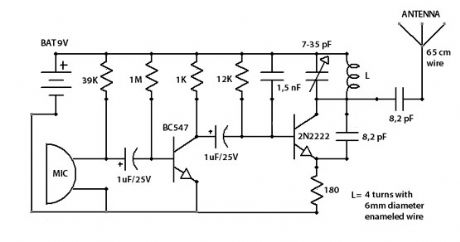
This easy to build FM transmitter bug can transmit voice to exceptionally good range. Tune trimmer to hear the signal to your near radio. Transmitter frequency range is 88-108 MHz. Max current consumption is 30mA. You can power the fm transmitter bug with a 9Volt Battery, or you can plug a power supply to feed in 9-12 Volts. That bug will pick even a low whisper or even the sound of a breath well far from the microphone. Great spy transmitter equipment. (View)
View full Circuit Diagram | Comments | Reading(1742)
SAA1057 PLL Synthesized FM Transmitter
Published:2012/11/15 0:56:00 Author:muriel | Keyword: SAA1057, PLL, Synthesized, FM , Transmitter
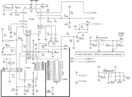
The functioning of all is provided by a microcontroller from MICROCHIP PIC16F84 which provides support for buttons, LCD 2 lines of 16 characters and the circuit pll SAA1057. The VCO is entrusted to the transistor Q8 associate of his two diodes varicaps BB109, a floor buffer Q7 separates the VHF signal obtained in two ways, on the one hand to Q9 to enslave loop phase and on the other hand to the Q5 and Q6 together which takes care to amplify the signal before attacking Q11, a BFR96 which plays the role of HF switch via a timer NE555 which receives information from the push and SAA1057 ensuring HF cutoff in the event of failure of a locking or unlocking of the pll. (View)
View full Circuit Diagram | Comments | Reading(4354)
RF Buffer Stage
Published:2012/11/15 0:46:00 Author:muriel | Keyword: RF , Buffer Stage
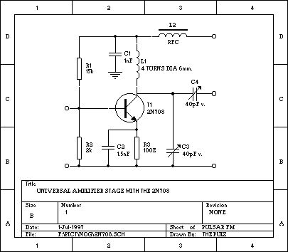
This bufferstage is intended to be used after a BF900 or BF199 (even a BF245) oscillator. It delivers several milliwatts and is perfect to drive a 2N2219 or 2N4427. Be sure the coils are really round and can see each other: place metalplates between the coils. The supply voltage is around 12V (typ. 13,8V). (View)
View full Circuit Diagram | Comments | Reading(4107)
Ramsey 25 BA1404 Stereo FM Transmitter
Published:2012/11/15 0:45:00 Author:muriel | Keyword: Ramsey , 25 , BA1404 , Stereo , FM, Transmitter
Stereo FM transmitter based on BA1404 and 145170 frequency synthesizer IC. (View)
View full Circuit Diagram | Comments | Reading(4537)
Prescaler with Counter
Published:2012/11/15 0:43:00 Author:muriel | Keyword: Prescaler , Counter
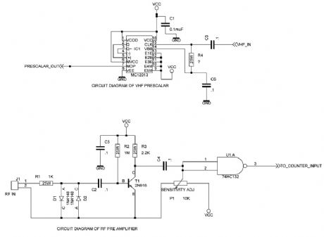
Digital frequency counter is being used for wide range of applications. Digital frequency counter extensively uses digital circuits and hence fairly good knowledge of digital circuits and of digital integrated circuits is required to understand the operation of the frequency counter. However a person who is not familiar with any electronics circuits and experiments has in written this article. (View)
View full Circuit Diagram | Comments | Reading(1542)
PLL Stereo FM Transmitter
Published:2012/11/15 0:41:00 Author:muriel | Keyword: PLL, Stereo , FM, Transmitter
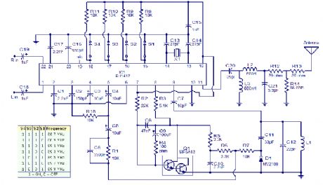
The circuit shown here is of a good Stereo FM transmitter that can transmit high quality signals up to a range of 70 feet. The circuit is based on BH1417 PLL stereo transmitter IC from Rhom semiconductors. The IC has separate audio processing sections for the left and right channels, pre emphasis circuit for improving signal to noise ratio, crystal control circuitry for accurate frequency locking, multiplex circuit for making sum ( left plus right) and difference ( left minus right) {see this article for better understanding Stereo decoder circuit} etc. Another important feature of this IC is that the transmission frequency can be set using a 4 channel DIP switch. The IC can be powered from anything between 4 to 6V DC and has an output power around 20mW. At full output power the circuit consumes only 20mA and has a channel separation of 40dB.There are 14 possible preset transmission frequencies, starting from 88.7MHz and incrementing in steps of 0.2MHz that can be selected using the DIP switch. The PLL circuitry of the IC is so precise that there is practically no frequency drift.
Circuit Description Capacitors C18 and C19 are DC decoupling capacitors for the left and right channel inputs. Capacitors C1 and C17 are used to set the amount of pre-emphasis required and here with the used values it is 50uS. Capacitors C2 and C16 sets the roll-off point of the low pass filter. The crystal X1 is a 7.6MHz crystal which sets the oscillator抯 frequency while capacitors C13 and C14 associated with are used for providing the appropriate loading. Resistors R8 to R11 are the pull-up resistors for the D0 to D3 (pins 15 to 18 of the IC) respectively. These pins can be held low by closing the corresponding switches. The RF oscillator of the IC is tuned using the components L1, C11, C12 and D1. Capacitor C11 prevents and DC voltage being applied to the varicap diode D1 and thereby prevents current flow into the inductor L1. More over it reduces the effects of changes in the capacitance of D1 on the pin 9. Capacitor C7 prevents any DC current from flowing into the inductor L1 from pin 9 of the IC. The composite output signal at pin 5 is applied to the junction of R6 and R7 though a network comprising of components C4, C5, C6 and R1. In the circuit pin 19 of the circuit is left unconnected, but an optional capacitor at this pin can be used to set the pilot level and phase. Any way such a capacitor is not at all a necessity here and the circuit will work perfectly even if the capacitor at pin 9 is omitted. The composite output signal undergoes some attenuation while passing through this network and finally reaches the varicap diode D1. The carrier frequency is controlled using the PLL (phase lock loop) phase detector output pin (pin 7) and the components connected around it. The darlington transistor Q1 is driven by the output of the pin7 and the transistor applies a control voltage on the varicap diode through resistor R5, R6 and R7. Capacitor C10 works as a high frequency filter while R7 is meant for isolation. Resistor R4 and capacitor C9 connected in series between the collector and base of Q1 provides further filtering. Resistor R4 improves the response of the transistor to transient changes while capacitor C9 improves low frequency filtering. Capacitor C8 connected between collector and base of Q1 provides additional high frequency filtering. Resistor R3 serves as the collector load for the transistor Q1. The modulated RF output is available at pin 11 and it is fed to the antenna through a filter network consisting of components L2, L3, C20, and C21. The job of this filter network is to remove harmonics. Resistors R12, R13 and R14 reduces the signal level to the antenna and as a result decreases the output power of the transmitter. Such a reduction is necessary to make the transmitter legal because in many countries transmitters that has an output power more than few milli watts (may change from nation to nation) are illegal. By omitting R12, R13, R14 and connecting the antenna directly to the junction of L2 and C21, the range can be increased, but do it at your own risk. Setting up the transmitter. Firstly set the frequency of transmission using the DIP switch. Then connect the circuit to the power supply and connect the positive lead of your multimeter to pin 8 of the IC and the negative lead to ground. The multimeter should show a reading equal to the supply voltage. Now move the positive lead of the multimeter to the junction of R5 and R6 and adjust the slug (ferrite core of L1) so that the multimeter reads 2V. The L1 has to be readjusted for getting 2V between junction of R5, R6 and Ground every time you change the transmission frequency. (View)
View full Circuit Diagram | Comments | Reading(3547)
PLL FM Transmitter using LMX1601, ATtiny2313 AT90S2313
Published:2012/11/15 0:37:00 Author:muriel | Keyword: PLL, FM Transmitter, LMX1601, ATtiny2313, AT90S2313
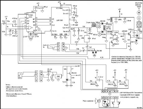
Here's a PLL FM Transmitter using LMX1601, ATtiny2313 or AT90S2313 microcontrollers. The common characteristic of all of the previous low power FM transmitters I've built over the decades, is that their operating frequency is determined by an LC resonant circuit. Some of them had excellent stability, some of them didn't, but I had always wanted to make one that is crystal controlled. Various schemes had been considered from time-to-time, including the direct approach of modulating the load capacitance of a a crystal oscillator, a whimsical phase modulation scheme involving a phase shifter, some balanced modulators, and limiting amplifiers, and at times, the down-to-earth and sober approach of modulating a VCO within a phase locked loop (PLL). While browsing Digikey's online catalog, I found the LMX1601 frequency synthesizer chip and thought: Just maybe, the PLL approach is finally within my grasp. The LMX1601, which apparently was designed for use in cell phones, includes everything need to make two phase locked loops except for the VCOs. More importantly, one of the PLLs, specifically the AUX PLL, is specified to work in the FM broadcast band. The LMX1600 and the LMX1602 were also considered, but the LMX1601 was selected because it has a 500 MHz option , meaning that it can work down to about 50 MHz.
An LMX1601 Phase locked loop, a discreet FET VCO, and an AVR micro controller combine to make a stable, easy to use monophonic FM transmitter that includes a an audio activated switch that turns the transmitter on only when its being used. With the LED lit blue to indicate the transmit mode, the transmitter's user interface is clean and simple. Two push buttons step the frequency up and down. The transmitter comes one when audio of sufficient amplitude is applied, and stays on for five minutes after the audio drops below the threshold. The LED flashes red briefly to show when audio is detected, so I know if the volume of the audio signal is high enough. A small hole under the LED is for the piezoelectric transducer, whose main job is to produce key clicks when the frequency increment and decrement buttons are pressed. The buttons do not provide tactile feedback. The painful part was dealing with the packaging of the chip. The lead centers of this 16 pin package are only 0.65 mm apart. Dealing with the fine printed circuit board features that would be needed to mount this chip was the most daunting aspect of using the chip. I had only experimented with the laser printer toner etch resist method of making PC boards a few months earlier, with some success. As it turned out, the laser printer toner etch resist method could be pushed to make a board that supports this chip. But just barely. (View)
View full Circuit Diagram | Comments | Reading(2955)
| Pages:29/195 At 202122232425262728293031323334353637383940Under 20 |
Circuit Categories
power supply circuit
Amplifier Circuit
Basic Circuit
LED and Light Circuit
Sensor Circuit
Signal Processing
Electrical Equipment Circuit
Control Circuit
Remote Control Circuit
A/D-D/A Converter Circuit
Audio Circuit
Measuring and Test Circuit
Communication Circuit
Computer-Related Circuit
555 Circuit
Automotive Circuit
Repairing Circuit